
Datasheet


5/15
TDA7296
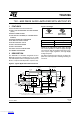
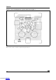
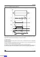
3 APPLICATION SUGGESTIONS
(see Test and Application Circuits of the Fig. 2)
The recommended values of the external components are those shown on the application circuit of Figure
2. Different values can be used; the following table can help the designer.
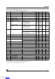
(*) R1 = R3 for pop optimization
(**) Closed Loop Gain has to be ≥ 24dB
COMPONENTS
SUGGESTED
VALUE
PURPOSE
LARGER THAN
SUGGESTED
SMALLER THAN
SUGGESTED
R1 (*) 22k Input Resistance Increase Input
Impedance
Decrease Input
Impedance
R2 680Ω Closed Loop Gain
Set to 30db (**)
Decrease of Gain Increase of Gain
R3 (*) 22k Increase of Gain Decrease of Gain
R4 22k St-by Time Constant Larger St-by
ON/OFF Time
Smaller St-by ON/OFF
Time; Pop Noise
R5 10k Mute Time Constant Larger Mute
ON/OFF Time
Smaller Mute
ON/OFF Time
C1 0.47µF Input DC Decoupling Higher Low Frequency
Cutoff
C2 22µF Feedback DC
Decoupling
Higher Low Frequency
Cutoff
C3 10µF Mute Time Constant Larger Mute
ON/OFF Time
Smaller Mute ON/OFF
Time
C4 10µF St-by Time Constant Larger St-by
ON/OFF Time
Smaller St-by ON/OFF
Time; Pop Noise
C5 22µF Bootstrapping Signal Degradation at
Low Frequency
C6, C8 1000µF Supply Voltage Bypass Danger of Oscillation
C7, C9 0.1µF Supply Voltage Bypass Danger of Oscillation
Downloaded from Arrow.com.Downloaded from Arrow.com.Downloaded from Arrow.com.Downloaded from Arrow.com.Downloaded from Arrow.com.