
Datasheet


Table Of Contents
- Figure 1. Internal schematic diagram
- Table 1. Device summary
- 1 Electrical ratings
- 2 Electrical characteristics
- Table 5. On/off states
- Table 6. Dynamic
- Table 7. Switching times
- Table 8. Source drain diode
- 2.1 Electrical characteristics (curves)
- Figure 2. Safe operating area
- Figure 3. Thermal impedance
- Figure 4. Output characteristics
- Figure 5. Transfer characteristics
- Figure 6. Normalized BVDSS vs temperature
- Figure 7. Static drain-source on resistance
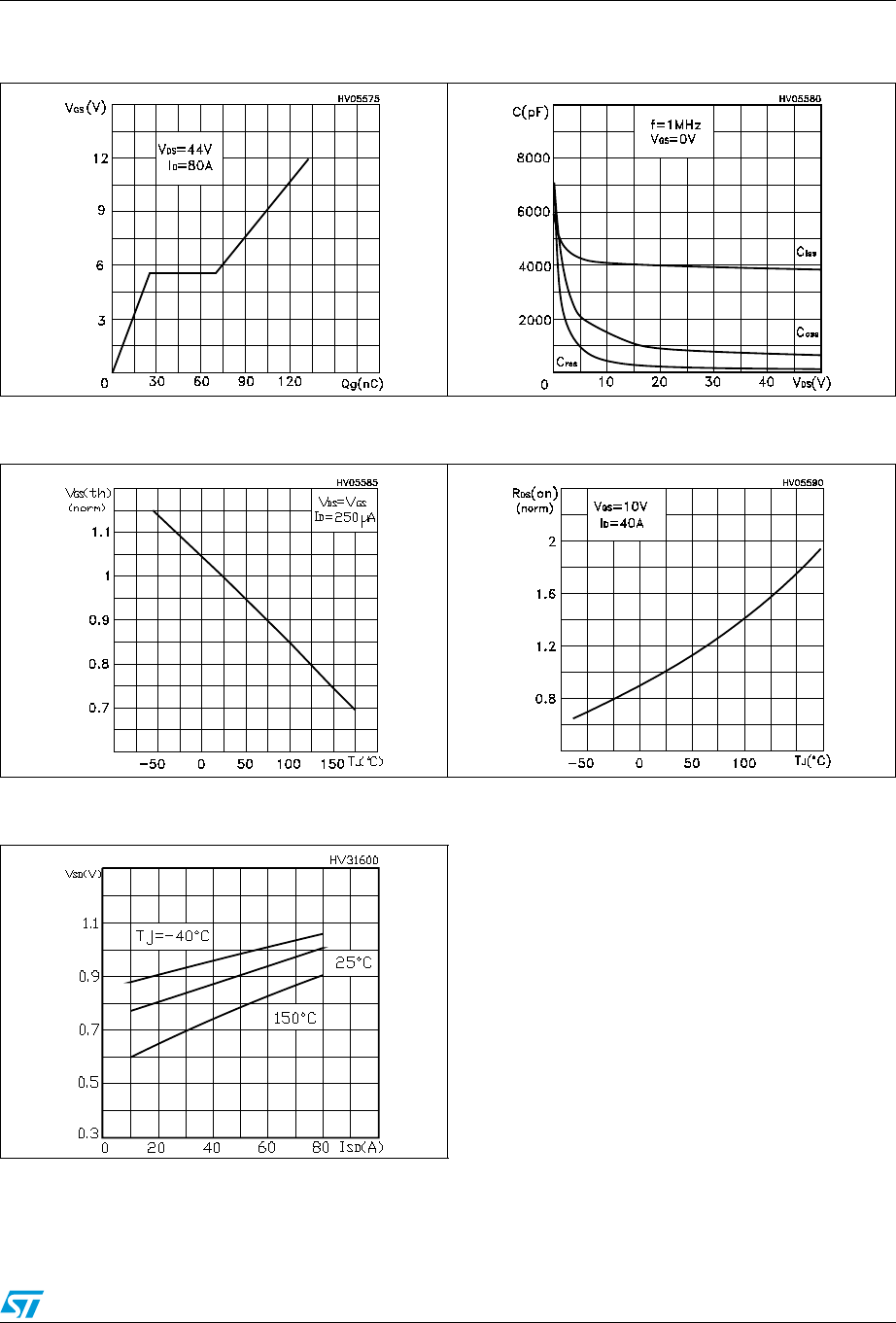
- Figure 8. Gate charge vs gate-source voltage
- Figure 9. Capacitance variations
- Figure 10. Normalized gate threshold voltage vs temperature
- Figure 11. Normalized on resistance vs temperature
- Figure 12. Source-drain diode forward characteristics
- 3 Test circuits
- 4 Package mechanical data
- 5 Packaging mechanical data
- 6 Revision history
STB80NF55-08T4, STP80NF55-08, STW80NF55-08 Electrical characteristics
Doc ID 14511 Rev 2 7/15
Figure 8. Gate charge vs gate-source voltage Figure 9. Capacitance variations
Figure 10. Normalized gate threshold voltage
vs temperature
Figure 11. Normalized on resistance vs
temperature
Figure 12. Source-drain diode forward
characteristics