
Datasheet


DocID026284 Rev 4 53/128
STM32F091xB STM32F091xC Electrical characteristics
99
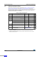
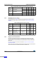
Table 22. Current characteristics
Symbol Ratings Max. Unit
I
VDD
Total current into sum of all VDD power lines (source)
(1)
120
mA
I
VSS
Total current out of sum of all VSS ground lines (sink)
(1)
-120
I
VDD(PIN)
Maximum current into each VDD power pin (source)
(1)
100
I
VSS(PIN)
Maximum current out of each VSS ground pin (sink)
(1)
-100
I
IO(PIN)
Output current sunk by any I/O and control pin 25
Output current source by any I/O and control pin -25
I
IO(PIN)
Total output current sunk by sum of all I/Os and control pins
(2)
80
Total output current sourced by sum of all I/Os and control pins
(2)
-80
Total output current sourced by sum of all I/Os supplied by VDDIO2 -40
I
INJ(PIN)
(3)
Injected current on FT and FTf pins -5/+0
(4)
Injected current on TC and RST pin ± 5
Injected current on TTa pins
(5)
± 5
I
INJ(PIN)
Total injected current (sum of all I/O and control pins)
(6)
± 25
1. All main power (VDD, VDDA) and ground (VSS, VSSA) pins must always be connected to the external power supply, in the
permitted range.
2. This current consumption must be correctly distributed over all I/Os and control pins. The total output current must not be
sunk/sourced between two consecutive power supply pins referring to high pin count QFP packages.
3. A positive injection is induced by V
IN
> V
DDIOx
while a negative injection is induced by V
IN
< V
SS
. I
INJ(PIN)
must never be
exceeded. Refer to Table 21: Voltage characteristics for the maximum allowed input voltage values.
4. Positive injection is not possible on these I/Os and does not occur for input voltages lower than the specified maximum
value.
5. On these I/Os, a positive injection is induced by V
IN
> V
DDA
. Negative injection disturbs the analog performance of the
device. See note
(2)
below Table 59: ADC accuracy.
6. When several inputs are submitted to a current injection, the maximum
I
INJ(PIN)
is the absolute sum of the positive and
negative injected currents (instantaneous values).
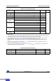
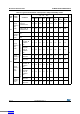
Table 23. Thermal characteristics
Symbol Ratings Value Unit
T
STG
Storage temperature range –65 to +150 °C
T
J
Maximum junction temperature 150 °C
Downloaded from Arrow.com.Downloaded from Arrow.com.Downloaded from Arrow.com.Downloaded from Arrow.com.Downloaded from Arrow.com.Downloaded from Arrow.com.Downloaded from Arrow.com.Downloaded from Arrow.com.Downloaded from Arrow.com.Downloaded from Arrow.com.Downloaded from Arrow.com.Downloaded from Arrow.com.Downloaded from Arrow.com.Downloaded from Arrow.com.Downloaded from Arrow.com.Downloaded from Arrow.com.Downloaded from Arrow.com.Downloaded from Arrow.com.Downloaded from Arrow.com.Downloaded from Arrow.com.Downloaded from Arrow.com.Downloaded from Arrow.com.Downloaded from Arrow.com.Downloaded from Arrow.com.Downloaded from Arrow.com.Downloaded from Arrow.com.Downloaded from Arrow.com.Downloaded from Arrow.com.Downloaded from Arrow.com.Downloaded from Arrow.com.Downloaded from Arrow.com.Downloaded from Arrow.com.Downloaded from Arrow.com.Downloaded from Arrow.com.Downloaded from Arrow.com.Downloaded from Arrow.com.Downloaded from Arrow.com.Downloaded from Arrow.com.Downloaded from Arrow.com.Downloaded from Arrow.com.Downloaded from Arrow.com.Downloaded from Arrow.com.Downloaded from Arrow.com.Downloaded from Arrow.com.Downloaded from Arrow.com.Downloaded from Arrow.com.Downloaded from Arrow.com.Downloaded from Arrow.com.Downloaded from Arrow.com.Downloaded from Arrow.com.Downloaded from Arrow.com.Downloaded from Arrow.com.Downloaded from Arrow.com.