
Datasheet

Hardware specifications SPSGRF
10/24 DocID027664 Rev 6
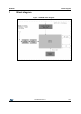
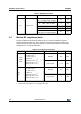
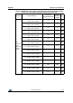
3.6 Pin connections
Figure 3. Pin connection diagram
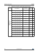
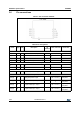
Table 9. Pin assignment
Name Type Pin# Description
Alt
function
V max. tolerance Initial state
SPI interface
SPI_CLK I 7 SPI CLOCK (Max. 8 MHz) V
in
SPI_MISO O 8 SPI MISO (MASTER in / SLAVE out) V
in
SPI_MOSI I 9 SPI MOSI (MASTER out SLAVE in) V
in
SPI_CS I 10 SPI “Chip Select” (SPI slave select) V
in
Power and ground
V
in
5V
in
(1.8V - 3.6V max.)
GND 6 GND
Module shutdown
SDN I 11 Shutdown input (active high) (1.8V - 3.6V max.)
GPIO - general purpose input/output
GPIO [0] I/O 4
Programmable input / output &
analog temperature output
(1.8V - V
in
max.)
Digital output.
Low power
GPIO [1] I/O 3 Programmable input / output (1.8V - V
in
max.)
Digital output.
Low power
GPIO [2] I/O 2 Programmable input / output (1.8V - V
in
max.)
Digital output.
Low power
GPIO [3] I/O 1 Programmable input / output (1.8V - V
in
max.)
Digital output.
Low power