
Datasheet


Embedded functions register mapping LSM6DSL
96/114 DocID028475 Rev 7
10 Embedded functions register mapping
The tables given below provide a list of the first (A) and second (B) bank registers related to
the embedded functions available in the device and the corresponding addresses.
The embedded functions registers of bank A are accessible when FUNC_CFG_EN is set
to ‘1’ in FUNC_CFG_ACCESS (01h).
The embedded functions registers of bank B are accessible when both FUNC_CFG_EN
and FUNC_CFG_EN_B set to ‘1’ in FUNC_CFG_ACCESS (01h).
Note: All modifications of the content of the embedded functions registers have to be performed
with the device in power-down mode.
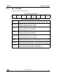
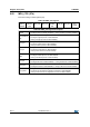
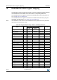
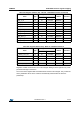
Table 223. Register address map - Bank A - embedded functions
Name Type
Register address
Default Comment
Hex Binary
SLV0_ADD r/w 02 00000010 00000000
SLV0_SUBADD r/w 03 00000011 00000000
SLAVE0_CONFIG r/w 04 00000100 00000000
SLV1_ADD r/w 05 00000101 00000000
SLV1_SUBADD r/w 06 00000110 00000000
SLAVE1_CONFIG r/w 07 00000111 00000000
SLV2_ADD r/w 08 00001000 00000000
SLV2_SUBADD r/w 09 00001001 00000000
SLAVE2_CONFIG r/w 0A 00001010 00000000
SLV3_ADD r/w 0B 00001011 00000000
SLV3_SUBADD r/w 0C 00001100 00000000
SLAVE3_CONFIG r/w 0D 00001101 00000000
DATAWRITE_SRC_
MODE_SUB_SLV0
r/w 0E 00001110 00000000
CONFIG_PEDO_THS_MIN r/w 0F 00001111 00010000
RESERVED - 10-12 Reserved
SM_THS r/w 13 00010011 00000110
PEDO_DEB_REG r/w 14 00010100 01101110
STEP_COUNT_DELTA r/w 15 0001 0101 00000000
MAG_SI_XX r/w 24 00100100 00001000
MAG_SI_XY r/w 25 00100101 00000000
MAG_SI_XZ r/w 26 00100110 00000000
MAG_SI_YX r/w 27 00100111 00000000
MAG_SI_YY r/w 28 00101000 00001000