
Datasheet


Register description LSM6DSL
52/114 DocID028475 Rev 7
9 Register description
The device contains a set of registers which are used to control its behavior and to retrieve
linear acceleration, angular rate and temperature data. The register addresses, made up of
7 bits, are used to identify them and to write the data through the serial interface.
9.1 FUNC_CFG_ACCESS (01h)
Enable embedded functions register (r/w).
Table 21. FUNC_CFG_ACCESS register description
9.2 SENSOR_SYNC_TIME_FRAME (04h)
Sensor synchronization time frame register (r/w).
Table 24. SENSOR_SYNC_TIME_FRAME register description
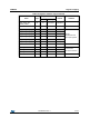
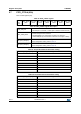
Table 20. FUNC_CFG_ACCESS register
FUNC_
CFG_EN
0
(1)
1. This bit must be set to ‘0’ for the correct operation of the device.
FUNC_
CFG_EN_B
0
(1)
0
(1)
0
(1)
0
(1)
0
(1)
FUNC_CFG_
EN
Enable access to the embedded functions configuration registers bank A and B
(1)
.
Default value: 0. Refer to Table 22.
1. The embedded functions configuration registers details are available in Section 10: Embedded functions
register mapping, Section 11: Embedded functions registers description - Bank A, and Section 12:
Embedded functions registers description - Bank B.
FUNC_CFG_
EN_B
Enable access to the embedded functions configuration register bank B
(1)
.
Default value: 0. Refer to Table 22.
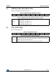
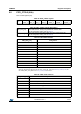
Table 22. Configuration of embedded functions register banks
FUNC_CFG_EN FUNC_CFG_EN_B Status of embedded register banks
0 0 Bank A and B disabled (default)
0 1 Forbidden
1 0 Bank A enabled
1 1 Bank B enabled
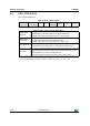
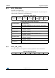
Table 23. SENSOR_SYNC_TIME_FRAME register
0
(1)
1. This bit must be set to ‘0’ for the correct operation of the device.
0
(1)
0
(1)
0
(1)
TPH_3 TPH_2 TPH_1 TPH_0
TPH_ [3:0]
Sensor synchronization time frame with the step of 500 ms and full range of 5 s.
Unsigned 8-bit.
Default value: 0000 0000 (sensor sync disabled)