
Datasheet


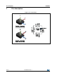


Pin description LSM6DSL
20/114 DocID028475 Rev 7
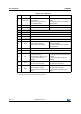
Table 2. Pin description
Pin# Name Mode 1 function Mode 2 function
1 SDO/SA0
SPI 4-wire interface serial data
output (SDO)
I
2
C least significant bit of the
device address (SA0)
SPI 4-wire interface serial data output
(SDO)
I
2
C least significant bit of the device
address (SA0)
2 SDx Connect to VDDIO or GND I
2
C serial data master (MSDA)
3 SCx Connect to VDDIO or GND I
2
C serial clock master (MSCL)
4 INT1 Programmable interrupt 1
5 VDDIO
(1)
1. Recommended 100 nF filter capacitor.
Power supply for I/O pins
6 GND 0 V supply
7 GND 0 V supply
8 VDD
(1)
Power supply
9 INT2
Programmable interrupt 2
(INT2) / Data enable (DEN)
Programmable interrupt 2 (INT2)/
Data enable (DEN)/
I
2
C master external synchronization
signal (MDRDY)
10 NC
(2)
2. Leave pin electrically unconnected and soldered to PCB.
Leave unconnected
11 NC
(2)
Leave unconnected
12 CS
I
2
C/SPI mode selection
(1: SPI idle mode / I
2
C
communication enabled; 0: SPI
communication mode / I
2
C
disabled)
I
2
C/SPI mode selection
(1: SPI idle mode / I
2
C communication
enabled;
0: SPI communication mode / I
2
C
disabled)
13 SCL
I
2
C serial clock (SCL)
SPI serial port clock (SPC)
I
2
C serial clock (SCL)
SPI serial port clock (SPC)
14 SDA
I
2
C serial data (SDA)
SPI serial data input (SDI)
3-wire interface serial data output
(SDO)
I
2
C serial data (SDA)
SPI serial data input (SDI)
3-wire interface serial data output
(SDO)