
User's Manual

SPZB32W1A2.1 / SPZB32W1C2.1
6/12
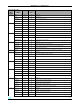
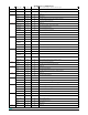
TIM2_CH4 I/O 24 Timer 2 channel 4 input / Timer 2 channel 4 output
11
GND -- 49 Ground
12
VDD Power 16,23,28,37 Input power supply
13
PC1 I/O 38 Digital I/O
ADC3 Analog 38 ADC Input 3
SWO O 38 Serial Wire Output ayncronous trace output to debugger
TRACEDATA0 O 38 Syncronous CPU trace data bit 0
14
PB0 I/O 36 Digital I/O
VREF (O/I) Analog 36 ADC reference output / ADC reference input
TIM1CLK I 36 Timer 1 external clock input
TIM2MSK I 36 Timer 2 external clock mask input
IRQA I 36 External interrupt source A
TRACECLK O 36 Syncronous CPU trace clock
15
PB1 I/O 30 Digital I/O
SC1TXD O 30 UART transmit data of Serial Controller 1
SC1MOSI /
SC1MISO
O 30 SPI master data out of Serial Controller 1 / SPI slave data out of Serial Controller 1
SC1SDA I/O 30 TWI (I2C) data of Serial Controller 1
TIM2_CH1 I/O 30 Timer 2 channel 1 input / Timer 2 channel 1 output
16
PB2 I/O 31 Digital I/O
SC1RXD I 31 UART receive data of Serial Controller 1
SC1MISO /
SC1MOSI
I 31 SPI master data in of Serial Controller SC1 / SPI slave data in of Serial Controller 1
SC1SCL I/O 31 TWI (I2C) clock of Serial Controller 1
TIM2_CH2 I/O 31 Timer 2 channel 2 input / Timer 2 channel 2 output
17
JTCK I 32 JTAG clock input from debugger
SWCLK I/O 32 Serial Wire clock input/output with debugger
18
PC2 I/O 33 Digital I/O
JTDO O 33 JTAG data out to debugger
SWO O 33 Serial Wire Output asyncronous trace output to debugger
19
PC3 I/O 34 Digital I/O
JTDI I 34 JTAG data in from debugger
20
PC4 I/O 35 Digital I/O
JTMS I 35 JTAG mode select from debugger
SWDIO I/O 35 Serial Wire bidirectional data to/from debugger
21
PC0 I/O 40 Digital I/O (high current)
JRST I 40 JTAG reset input from debugger
TRACEDATA1 O 40 Syncronous CPU trace data bit 1
IRQD I 40 External interrupt source D
22
PB7 I/O 41 Digital I/O
TIM1_CH2 O 41 Timer 1 channel 2 output
TIM1 _CH2 I 41 Timer 1 channel 2 input
IRQC I 41 External interrupt source C
ADC2 I 41 ADC input 2
23
PB6 I/O 42 Digital I/O