
User's Manual

SPZB32W1A2.1 / SPZB32W1C2.1
4/12
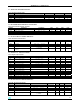
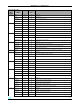
3 – ELECTRICAL CHARACTERISTICS
3.1 - ABSOLUTE MAXIMUM RATINGS
Table 1. Absolute maximum ratings
Symbol Parameter Min Max Unit
VDD Module supply voltage - 0.3 3.6 V
Vin Input voltage on any digital pin - 0.3 Vdd + 0.3 V
Tstg Storage tempeature -40 +85 °C
Tsold. Soldering temperature < 10s 250 °C
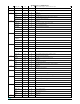
3.2 - RECOMMENDED OPERATING CONDITIONS
Table 2. Recommended operating conditions
Symbol Parameter Conditions Min Typ Max Unit
VDD Module supply voltage -40°C < T < +85 C 2.8 3.3 3.6 V
Tstg Operating ambient temperature -40 +85 °C
3.3 - DC ELECTRICAL CHARACTERISTICS
Table3. DC Electrical Characteristics
Symbol Parameter Conditions Min Typ Max Unit
IRX RX current Vdd = 3.3 V T= 25 °C 28 mA
ITX TX current Po = 3 dBm Vdd = 3.3 V T= 25 °C
F=2450 Mhz
32 mA
IDS Deep Sleep Current (32.768kHz
oscillator)
Vdd = 3.3 V T = 25°C 1.3
µΑ
3.4 - DIGITAL I/O SPECIFICATIONS
Table 4. Digital I/O Specifications
Symbol Parameter Conditions Min Typ Max Unit
VIL Low Level Input Voltage 2.8 < Vdd < 3.6 V 0 0.5 x
Vdd
V
VIH High level input voltage 2.8 < Vdd < 3.6 V 0.62 x Vdd Vdd V
Iil Input current for logic 0 2.8 < Vdd < 3.6 V -0.5
µΑ
Iih Input current for logic 1 2.8 < Vdd < 3.6 V 0.5
µΑ
Ripu Input pull-up resistor 30
κΩ
Ripd Input pull-down resistor 30
κΩ
VOL Low level output voltage 0 0.18 x
Vdd
V
VOH High level output voltage 0.82 x Vdd Vdd V
IOHS Output source current (standard ) 4 mA
IOLS Output sink current (standard) 4 mA
IOHH Output source current (high current) 8 mA
IOLH Output sink current (high current) 8 mA
IOTot Total output current for I/O 40 mA
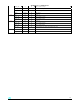
3.5 - RF ELECTRICAL CHARACTERISTICS
Table 5. RF Electrical Characteristics
Symbol Parameter Conditions Min Typ Max Unit
Frequency range Vdd = 3.3 V T= 25 °C 2405 2480 MHz
TX Output power Vdd = 3.3 V T= 25 °C 3 6 dBm
RX Sensitivity Vdd = 3.3V 1% PER -95 - 97 dBm
CFE Carrier frequency error Vd d= 3.3V -40 / + 85 °C
- t.b.d. t.b.d. ppm
Adjacent channel rejection +/- 5 MHz
+/- 10 MHZ
35
40
dBm