
User Manual
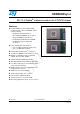
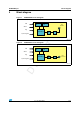
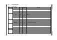
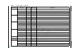
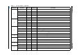
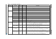
Table Of Contents
- 1 Description
- 2 RoHS compliance
- 3 Application
- 4 Block diagram
- 5 Pin settings
- 6 Electrical characteristics
- 7 Mechanical dimensions
- 8 Soldering
- 9 Product approvals
- 10 Ordering information scheme
- 11 Revision history

D
RAFT
SPZB32Wxy1.z Pin settings
Doc ID xxxxx Rev 1 9/19
14
PB0 I/O 36 Digital I/O
VREF (O/I) Analog 36 ADC reference output / ADC reference input
TIM1CLK I 36 Timer 1 external clock input
TIM2MSK I 36 Timer 2 external clock mask input
IRQA I 36 External interrupt source A
TRACECLK O 36 Syncronous CPU trace clock
15
PB1 I/O 30 Digital I/O
SC1TXD O 30 UART transmit data of Serial Controller 1
SC1MOSI / SC1MISO O 30 SPI master data out of Serial Controller 1 / SPI slave data out of Serial Controller 1
SC1SDA I/O 30 TWI (I2C) data of Serial Controller 1
TIM2_CH1 I/O 30 Timer 2 channel 1 input / Timer 2 channel 1 output
16
PB2 I/O 31 Digital I/O
SC1RXD I 31 UART receive data of Serial Controller 1
SC1MISO / SC1MOSI I 31 SPI master data in of Serial Controller SC1 / SPI slave data in of Serial Controller 1
SC1SCL I/O 31 TWI (I2C) clock of Serial Controller 1
TIM2_CH2 I/O 31 Timer 2 channel 2 input / Timer 2 channel 2 output
17
JTCK I 32 JTAG clock input from debugger
SWCLK I/O 32 Serial Wire clock input/output with debugger
18
PC2 I/O 33 Digital I/O
JTDO O 33 JTAG data out to debugger
SWO O 33 Serial Wire Output asyncronous trace output to debugger
19
PC3 I/O 34 Digital I/O
JTDI I 34 JTAG data in from debugger
20
PC4 I/O 35 Digital I/O
JTMS I 35 JTAG mode select from debugger
SWDIO I/O 35 Serial Wire bidirectional data to/from debugger
Table 1. Pin description (continued)
Module pin n° Pin name Direction STM32W pin Description