
User Manual
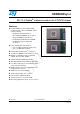
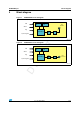
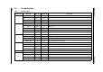
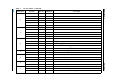
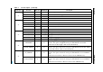
Table Of Contents
- 1 Description
- 2 RoHS compliance
- 3 Application
- 4 Block diagram
- 5 Pin settings
- 6 Electrical characteristics
- 7 Mechanical dimensions
- 8 Soldering
- 9 Product approvals
- 10 Ordering information scheme
- 11 Revision history

D
RAFT
Pin settings SPZB32Wxy1.z
10/19 Doc ID xxxxx Rev 1
21
PC0 I/O 40 Digital I/O (high current)
JRST I 40 JTAG reset input from debugger
TRACEDATA1 O 40 Syncronous CPU trace data bit 1
IRQD I 40 External interrupt source D
22
PB7 I/O 41 Digital I/O
TIM1_CH2 O 41 Timer 1 channel 2 output
TIM1 _CH2 I 41 Timer 1 channel 2 input
IRQC I 41 External interrupt source C
ADC2 I 41 ADC input 2
23
PB6 I/O 42 Digital I/O
TIM1_CH1 O 42 Timer 1 channel 1 output
TIM1_CH1 I 42 Timer 1 channel 1 input
IRQB I 42 External interrupt source B
ADC1 Analog 42 ADC input 1
24
LNA/ENABLE I 29
Digital input, module firmware dependent, externally forced by the user dedicated
firmware. This signal is dedicated to manage the SIGE-SE2432L internal LNA.
(HIGH= internal LNA enabled, LOW= internal LNA disabled).
PA6/LNA_ENABLE O 29
Digital output, module firmware dependent, internally forced by application dedicated
firmware. This signal is dedicated to manage the SIGE-SE2432L internal LNA. (HIGH=
internal LNA enabled, LOW= internal LNA disabled).
25
RF_STANDBY I 18
Digital input, module firmware dependent, externally forced by the user dedicated
firmware. This signal is dedicated to manage the SIGE-SE2432L front-end STANDBY
state.
(HIGH= Front-end enabled, LOW= Front-end forced in the STANDBY state).
PA7/RF_STANDBY O 18
Digital output, module firmware dependent, internally forced by application dedicated
firmware. This signal is dedicated to manage the SIGE-SE2432L front-end STANDBY
state.
(HIGH= Front-end enabled, LOW= Front-end forced into STANDBY state).
Table 1. Pin description (continued)
Module pin n° Pin name Direction STM32W pin Description