
User's Manual
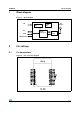
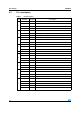
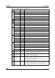
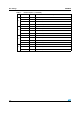
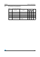
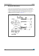
Table Of Contents

Pin settings SPZB250
4/16
2.2 Pin description
Table 1. Pin description
Pin n Pin name Direction Description
1
GPIO6 I/O Digital I/O
ADC2 Analog ADC input 2
TMR2CLK I External clock input of timer 2
TMR1ENMSK I External enable mask of timer1
2
GPIO5 I/O Digital I/O
ADC1 Analog ADC Input 1
PTI_DATA O Frame signal of PTI (Packet Trace Interface)
3
GPIO4 I/O Digital I/O
ADC0 Analog ADC Input 0
PTI_EN O Frame signal of PTI (Packet Trace Interface)
4
GPIO3 I/O Digital I/O
SSEL I SPI Master clock of Serial Controller SC2
TMR2IB.1 I Capture of Input B of timer 1
5 RSTB I Active low reset ( an internal pull-up of 30 kohm typ is provided)
6
GPIO11 I/O Digital I/O
CTS I UART CTS handshake of serial controller SC1
MCLK O SPI master clock of serial controller SC1
TMR2IA.1 I Capture of Input A of timer 2
7
GPIO12 I/O Digital I/O
RTS O UART RTS handshake of serial controller SC1
TMR2IB.1 I Capture of Input B of timer 2
8
GPIO0 I/O Digital I/O
MOSI O SPI master data out of serial controller SC2
MOSI I SPI slave data in of serial controller SC2
TMR1IA.1 I Capture of input A of timer 1
9
GPIO1 I/O Digital I/O
MISO I SPI master data in of serial controller SC2
MISO O SPI slave data out of serial controller SC2
SDA I/O I2C data of serial controller SC2
TMR2IA.2 I Capture of input A of timer 2