
User's Manual

SPWF04SA, SPWF04SC
Package information
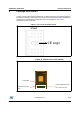
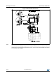
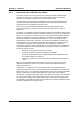
Figure 7. Wi-Fi module footprint
PCB design requires a detailed review of the center exposed pad. This pad requires good
thermal conductivity. Soldering coverage should be maximized and checked via x-ray for
proper design. There is a trade-off between providing enough soldering for conductivity and
applying too much, which allows the module to “float” on the paddle creating reliability
issues. ST recommends two approaches, a large center via that allows excess solder to
flow down into the host PCB with smaller vias around it, or many smaller vias with just
enough space for the viscosity of the chosen solder/flux to allow some solder to flow into the
smaller vias.
Either of these approaches must result in 60% or more full contact solder coverage on the
paddle after reflow. ST strongly encourages PCB layout teams to work with their EMS
providers to ensure vias and solder paste designs that will result in satisfactory
performance.
DocID025635 Rev 7 15/18