
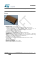
User's Manual


List of figures
February 2017
DocID0xxxxx Rev 0.xx 4/27
This is preliminary information on a new product now in development or undergoing evaluation. Details are subject to change
without notice. ww w.st.com
List of figures
Figure 1. Pin Placement (top view of LGA pads placed on bottom side).Errore. Il segnalibro non è definito.
Figure 2. Hardware block diagram ................................................................................................ 11
Figure 3. Typical application circuit of SPSGPE connected to a host microcontroller. ................... 13
Figure 4. Typical application circuit of SPSGPE connected to a host computer via USB. ............. 13
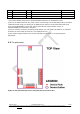
Figure 5. Example of SPSGPE layout. .......................................................................................... 13
Figure 6. Recommended SPSGPE footprint. ................................................................................ 18
Figure 7. Soldering profile. ............................................................................................................ 19
Figure 8. Package mechanical data…………………………………………………………… 21