
Data Sheet

SPBTLE-1S
P a g e | 12
Rev. 0.1
5 Hardware design
Note:
-
All unused pins should be left floating; do not ground.
-
GND pin must be well grounded.
-
Traces should not be routed underneath the module.
-
The area around the module should be free of any ground planes, power planes,
trace routings, or metal for 6 mm from the module antenna position, in all directions.
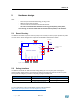
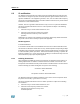
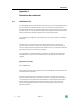
5.1 Reset Circuitry
The SPBTLE-1S module requires an external pull-up reset circuitry to ensure proper operation at power
on. Refer to the “Reset management” chapter of the BlueNRG-1 datasheet for details.
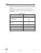
5.2 Debug Interface
The SPBTLE-1S
embeds the ARM serial wire debug (SWD) port. It is two pins (clock and single bi-
directional data) debug interface, providing all the debug functionality plus real time access to system
memory without halting the processor or requiring any target resident code.
Pin Functionality
Module PI
N
Pin description
SWCLK
12
SWD clock signal
SWDIO
13
SWD data signal
Table 5: Debug interface pin
For more information refer to the BlueNRG-1 technical documentation
(http://www.st.com/en/wireless-connectivity/bluenrg-1.html )
ANTENNA
BLE1
SPBTLE-1S MODULE
DIO11
11
DIO6
9
DIO7/BOOT
7
DIO8
10
VBAT
5
GND
8
ANATEST0/DIO14
6
DIO5
4
DIO4
3
ADC1
2
ADC2
1
DIO9
12
DIO10
13
(ANATEST1
14
DIO0
15
DIO2
16
DIO3
17
DIO1
18
RESETN
19
DIO12
20
GND_RF
21
EXT_ANT
22
GND_RF
23
C RESET
10nF
R RESET
47 KOHM
VCC (VBAT)
(IF NEEDED)
TO EXTERNAL CIRCUIT
Figure 7: Reset circuitry