
User's Manual

January
2016 DocID0xxxxx Rev 0.17
This is preliminary information on a new product now in development or undergoing evaluation. Details are subject to change
without notice. www.st.com
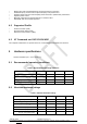
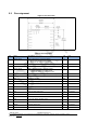
5.5 Pin assignment
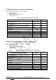
Table 5: Pin assignment
Pin
Name
Description
I/O
Note
1
GPIO1_BTCS
GPIO indicating BT Connection Status
- When high, BT connection is active
- When low, BT connection is not active
O
2
GPIO2
General purpose I/O
I/O
5V tolerant
3
GPIO3
General purpose I/O
I/O
5V tolerant
4
GPIO4_MLPS
GPIO indicating Module Low Power Status
- When high, device is in active mode
- When low, device is in low power mode
O
5
GPIO5 / I2C SDA
General purpose I/O or I2C_SDA line for MFI chip
I/O
5V tolerant
6
GPIO6 / I2C SCL
General purpose I/O or I2C_SCL line for MFI chip
I/O
5V tolerant
7
GND
Reference ground
NA
8
Vin
Main power supply input
NA
9
Boot 0
Boot 0 pin
I
5V tolerant
10
RESETn
Reset input (active low for 5ms)
I
11
CTS
Request to send (active low)
I
12
RTS
Clear to send (active low)
O
5V tolerant
13
RXD
Receive Data
I
5V tolerant
14
TXD
Transmit Data
O
15
LPO
Low power 32KHz oscillator input
I
16
GPIO7
General purpose I/O
I/O
5V tolerant
17
GPIO8
General purpose I/O
I/O
5V tolerant
18
+1.8V OUT
+1.8V out (max 10mA)
NA
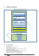
Figure 2: Pin connection