
User's Manual

Doc ID TBD Rev 0.8 Rev 0.1
3/19
www.st.com
List of tables
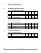
Table 1. Recommended operating conditions .................................................................................... 5
Table 2. Absolute maximum ratings ................................................................................................... 5
Table 3. I/O operating characteristics ................................................................................................. 5
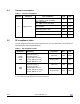
Table 4. Current consumption ............................................................................................................ 6
Table 5. RF compliance limits ............................................................................................................ 6
Table 6. Pin assignment ..................................................................................................................... 7
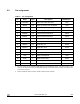
Table 7. Module pin usage ................................................................................................................. 9
Table 8. Soldering profile ................................................................................................................. 13
Table 12. Ordering information ....................................................................................................... 18
List of figures
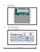
Figure 1. Pin placement ...................................................................................................................... 8
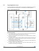
Figure 2. Hardware block diagram ...................................................................................................... 8
Figure 3. Typical application circuit ................................................................................................... 10
Figure 4. Layout guidelines ............................................................................................................... 11
Figure 5. Recommended footprint ..................................................................................................... 12
Figure 6. Soldering profile ................................................................................................................. 13
Figure 7. Mechanical data ................................................................................................................. 14