
User's Manual
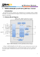
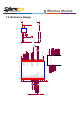
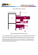
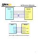
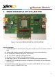
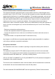
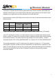
Table Of Contents

2
Wireless Module
Figure2. Module Reference Design
Figure3. Interface pin define reference design
The recommended schematic configuration for all of the interfaces and GPIOs are shown as
figure 4. The connection block diagram of the PCI-e interface is shown in figure 5. However,
the connection block diagram of UART and PCN interfaces is shown in figure 6. The PCI-e
differential pair signals impedance target is 100 ohms impedance. The length difference of
each pair of differential signals does not exceed 10 mil, and the integrity of a ground plane
should be maintained, as far as possible.
C5 NP
C7 NP
C6 NP
C8 NP
C12 NP
C10 NP
EXTERNAL 32KHz CLOCK
R7 NP/10K
WL_REG_ON
R8
NP/10K
C124 100pF
C123 100pF
R7 used for keep-alive.
VIO
VIO
R22 10K
R23 0R
R114 NP/0402/0R
32.768KHz
BT_HOST_WAKE
BT_WAKE
HOST_PCIE_CLKREQn PCIE_CLKREQn
C121 0.1uF
C122 0.1uF
R15 0R
R14 0R
VIO
BT_R ST_N
R8 used for keep-alive.
S_CLOCK
PCM_CLKHOST_PCM_CLK
BT_U AR T_R TS_NHOST_UART_CTS_N
BT_UART_RXDHOST_U ART_TXD
BT_U AR T_TXDHOST_UART_RXD
PCM_OUTHOST_PCM_IN
PCM_INHOST_PCM_OUT
PCM_SYNCHOST_PCM_SYNC
BT_U AR T_C TS_NHOST_UART_RTS_N
WL_HOST_WAKE
Connected to HOST I/O
WLAN
BT
R81
NP/10K
R80
NP/10K
HOST_PCIE_TDN
HOST_PCIE_TDP
HOST_PCIE_RDN
HOST_PCIE_RDP
HOST_PCIE_REFCLKP
PCIE_RDN
PCIE_RDP
PCIE_REFCLKP
PCIE_REFCLKN
PCIE_PRRST_L
VIO
PCIE_PME_L
R20 10K
R82
NC/10K
R21 0R
HOST_PCIE_PME_L
PCIE_TDP
PCIE_TDN
HOST_PCIE_REFCLKN