
Data Sheet
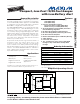

MAX17043/MAX17044
Compact, Low-Cost 1S/2S Fuel Gauges
with Low-Battery Alert
2 _______________________________________________________________________________________
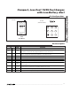
ABSOLUTE MAXIMUM RATINGS
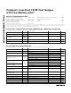
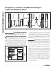
DC ELECTRICAL CHARACTERISTICS
(2.5V ≤ V
DD
≤ 4.5V, T
A
= -20°C to +70°C, unless otherwise noted. Contact Maxim for V
DD
greater than 4.5V.)
Stresses beyond those listed under “Absolute Maximum Ratings” may cause permanent damage to the device. These are stress ratings only, and functional
operation of the device at these or any other conditions beyond those indicated in the operational sections of the specifications is not implied. Exposure to
absolute maximum rating conditions for extended periods may affect device reliability.
Voltage on CTG Pin Relative to V
GND
....................-0.3V to +12V
Voltage on CELL Pin Relative to V
GND
...................-0.3V to +12V
Voltage on All Other Pins Relative to V
GND
..............-0.3V to +6V
Operating Temperature Range ...........................-40°C to +85°C
Storage Temperature Range
(T
A
= 0°C to +70°C (Note 10))........................-55°C to +125°C
Lead Temperature (TDFN soldering only, 10s) ...............+300°C
Soldering Temperature (reflow)
TDFN.............................................................................+260°C
UCSP.............................................................................+240°C
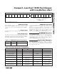
PARAMETER SYMBOL CONDITIONS MIN TYP MAX UNITS
Active Current I
ACTIVE
50 75 µA
V
DD
= 2.0V 0.5 1.0
Sleep-Mode Current (Note 2) I
SLEEP
1 3
µA
V
DD
= 3.6V at +25°C -1 +1
T
A
= 0°C to +70° C (Note 10) -2 +2
Time-Base Accuracy t
ERR
T
A
= -20°C to +70°C -3 +3
%
T
A
= +25°C, V
IN
= V
DD
-12.5 +12.5
MAX17043 Voltage-
Measurement Error
-30 +30
mV
T
A
= +25°C, 5.0V < V
IN
< 9.0V -30 +30
MAX17044 Voltage-
Measurement Error
V
GERR
5.0 < V
IN
< 9.0 -60 +60
mV
CELL Pin Input Impedance R
CELL
15 M
Input Logic-High:
SCL, SDA, QSTRT
V
IH
(Note 1) 1.4 V
Input Logic-Low:
SCL, SDA, QSTRT
V
IL
(Note 1) 0.5 V
Output Logic-Low: SDA V
OL
I
OL
= 4mA (Note 1) 0.4 V
Output Logic-Low: ALRT V
OL-ALRT
I
OL-ALRT
= 2mA (Note 1) 0.4 V
Pulldown Current: SCL, SDA I
PD
V
DD
= 4.5V, V
PIN
= 0.4V 0.2 µA
Input Capacitance: SCL, SDA C
BUS
50 pF
Bus Low Timeout t
SLEEP
(Note 3) 1.75 2.5 s
Mode Transition t
TRAN
(Note 4) 1 ms
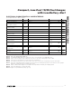
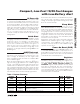
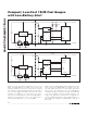
ELECTRICAL CHARACTERISTICS RECOMMENDED DC OPERATING CONDITIONS
(2.5V ≤ V
DD
≤ 4.5V, T
A
= -20°C to +70°C, unless otherwise noted.)
PARAMETER SYMBOL CONDITIONS MIN TYP MAX UNITS
Supply Voltage V
DD
(Note 1) +2.5 +4.5 V
Data I/O Pins
SCL, SDA,
QSTRT,
ALRT
(Note 1) -0.3 +5.5 V
MAX17043 CELL Pin V
CELL
(Note 1) -0.3 +5.0 V
MAX17044 CELL Pin V
CELL
(Note 1) -0.3 +10.0 V