
Data Sheet

NAU7802 24-bit ADC
Nuvoton Confidential - 35 - Revision 1.7
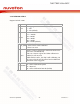
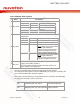
11.10 REG0x15: ADC registers
Bit
Name
Description
5:4
REG_CHPS
Select the CLK_CHP clock frequency.
REG_CPHS[1]
REG_CPHS[0]
CLK_CHP clock frequency
0
0
Reserved
0
1
Reserved
1
0
Reserved
1
1
turned off, high ('1') state
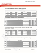
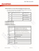
3:2
ADC_VCM
Select the ADC input common mode for unipolar
configuration.
ADC_VCM[1]
ADC_VCM[0]
CHP_CLKSD Delay
0
0
disable
0
1
disable
1
0
Enable extended common mode.
When voltage range close to REFN
with ADC gain divided by 2.
Reduced common mode rejection.
Requires PGA bypass mode set.
1
1
Enable extended common mode.
When voltage range close to REFP
with ADC gain divided by 2.
Reduced common mode rejection.
Requires PGA bypass mode set
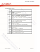
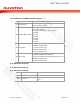
1:0
REG_CHP
Select delay between ADC clock (CLKSD) and ADC
chopper clock (CHP_CLKSD).
Clock delay variance between Chopper and ADC sections can
improve linearity of the application.
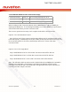
Issue an I2C write REG0x15 with write data will update the ADC registers.
For reading back ADC registers, make sure REG0x1B[7] RD_OTP_SEL=0 (default), then
issue a I2C read REG0x15 to read ADC registers
ADC registers and OTP[32:24] are sharing REG0x15 when read back, the REG0x1B[7]
RD_OTP_SEL (default 0) is used as read select
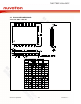
REG0x15
Read
REG0x1B[7]=RD_OTP_SEL=1
Read back OTP[32:24]
REG0x15
Read
REG0x1B[7]=RD_OTP_SEL=0(default)
Read back ADC
Registers(default)