
Data Sheet

NAU7802 24-bit ADC
Nuvoton Confidential - 25 - Revision 1.7
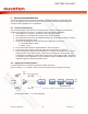
9 APPLICATION INFORMATION
This section includes both circuit diagram information and recommendations for programming the
device. Programming is essential, as the device will not function until various default settings are
changed to values appropriate for the application.
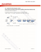
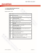
9.1 Power-On Sequencing
After the DVDD supply is valid, and after the internal power-on reset is completed, the NAU7802 is
ready for host program control access. The following steps apply to most applications.
1. Set the RR bit to 1 in R0x00, to guarantee a reset of all register values.
2. Set the RR bit to 0 and PUD bit 1, in R0x00, to enter normal operation
3. After about 200 microseconds, the PWRUP bit will be Logic=1 indicating the device is ready for
the remaining programming setup.
4. At this point, all appropriate device selections and configuration can be made.
a. For example R0x00 = 0xAE
b. R0x15 = 0x30
5. No conversion will take place until the R0x00 bit 4 “CS” is set Logic=1
6. Enter the low power standby condition by setting PUA and PUD bits to 0, in R0x00
7. Resume operation by setting PUA and PUD bits to 1, in R0x00. This sequence is the same for
powering up from the standby condition, except that from standby all of the information in the
configuration and calibration registers will be retained if the power supply is stable. Depending
on conditions and the application, it may be desirable to perform calibration again to update the
calibration registers for the best possible accuracy.
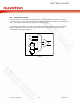
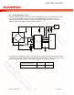
9.2 Signal path normal operation
In normal operation the input signal is full scale at the ADC input when
(VINxP - VINxN) = +/- 0.5 * (REFP - REFN) / PGA_Gain, within the PGA common mode range.