NAU7802 24-bit ADC NAU7802 24-Bit Dual-Channel ADC For Bridge Sensors Date: January, 2012 Revision 1.7 Nuvoton Confidential -1- Revision 1.
NAU7802 24-bit ADC Table of Contents 1 2 3 4 5 6 7 GENERAL DESCRIPTION ......................................................................................................... 4 SYSTEM BLOCK DIAGRAM ...................................................................................................... 4 FEATURES ................................................................................................................................. 4 APPLICATIONS ...................................................
NAU7802 24-bit ADC 10 11 9.4 16-pin application circuit ............................................................................................... 27 SUMMARY DEVICE REGISTER MAP ..................................................................................... 28 DEVICE REGISTER MAP DETAILS......................................................................................... 29 11.1 REG0x00:PU_CTRL .................................................................................................
NAU7802 24-bit ADC 1 GENERAL DESCRIPTION The Nuvoton NAU7802 is a precision low-power 24-bit analog-to-digital converter (ADC), with an onboard low-noise programmable gain amplifier (PGA), onboard RC or Crystal oscillator, and a precision 24-bit sigma-delta (Σ-Δ) analog to digital converter (ADC). The NAU7802 device is capable of up to 23-bit ENOB (Effective Number Of Bits) performance.
NAU7802 24-bit ADC 3 4 FEATURES Supply power: 2.7V~5.5V On-chip VDDA regulator for internal analog circuit or external load cell Programmable VDDA: Off, 2.4V to 4.5V with eight options Minimum 10mA output drive capability at 3.0V output voltage Note: DVDD must be 0.
NAU7802 24-bit ADC 5 6 PIN CONFIGURATION REFP 1 16 AVDD/LDO VIN1N 2 15 DVDD VIN1P 3 14 SDIO 13 SCLK 12 DRDY 11 XOUT XIN SOP-16 (150mil) or DIP-16 VIN2N 4 VIN2P 5 VBG 6 REFN 7 10 AVSS 8 9 DVSS PIN DESCRIPTION Pin No.
NAU7802 24-bit ADC 7 7.1 ELECTRICAL CHARACTERISTICS Absolute Maximum Ratings SYMBOL PARAMETER CONDITION MINIMUM MAXIMUM UNIT DVDD DVDDDVSS -0.3 +6.0 V AVDD* AVDDAVSS -0.3 +6.0 V AVSSDVSS - -0.3 +0.3 V Analog Input Voltage AVIN AVIN AVSS -0.3 AVDD + 0.3 V Digital input Voltage DVIN DVIN DVSS -0.3 DVDD + 0.
NAU7802 24-bit ADC ANALOG INPUT Full-scale input range (VINxP – VINxN) ± 0.5/(VREF/PGA) V Common mode range with PGA gain 64, 128 AVSS + 1.5 AVDD – 1.5 V Common mode range with PGA bypass enabled AVSS 0.1 AVDD + 0.1 V Differential input impedance Bandwidth (-3dB) PGA VREF = REFP REFN 5 GΩ PGA bypass=off, DC 2.27 Hz Data output rate = 10 SPS Hz Data output rate = 80 SPS 18.
NAU7802 24-bit ADC DIGITAL SERIAL INTERFACE Input Leakage Current SCK, SI Input High Voltage VIH -1 - +1 A DVDD = 5.5V, 0
NAU7802 24-bit ADC 7.5 Typical Characteristic 7.5.1 NAU7802 Linearity – (Error % vs. Input Voltage) AVDD = 4.5V / PGA gain = 1x 0.0008 0.0006 0.0004 0 -1.2 -1 -0.8 -0.6 -0.4 -0.2 -0.0002 0 -0.0004 -0.0006 -0.0008 Error (% of FS) 0.0002 0.2 -0.001 -0.0012 Input Signal Voltage (V : VINP - VINN) NAU7802 Linearity Performance is symmetric, from the differential input voltage -1.2V to 0V and from 0V to 1.2V. One-sided linearity performance result is shown.
NAU7802 24-bit ADC 7.5.2 Noise Performance – NAU7802 7.5.3 ESD Performance – NAU7802 Zapping Method PD PS ND NS Remark HBM 4kV 4kV -4kV -4kV Pass MM 400V 400V -400V -400V Pass Nuvoton Confidential - 11 - Revision 1.
NAU7802 24-bit ADC 7.
NAU7802 24-bit ADC 8 8.1 FUNCTIONAL DESCRIPTION Analog input (VIN1P, VIN1N, VIN2N, VIN2P) The input signal to be measured is applied to one of two differential input signal pairs. The desired signal pair is selected using an analog input multiplexer, which is controlled by settings in the device command and control registers. The 8-pin version of the device supports only one input signal pair. This device is optimized to accept differential input signals, but can also measure single-ended signals.
NAU7802 24-bit ADC 8.3.1 2-Wire Protocol Convention All 2-Wire interface operations must begin with a START condition, which is a HIGH-to-LOW transition of SDIO while SCLK is HIGH. All 2-Wire interface operations are terminated by a STOP condition, which is a LOW to HIGH transition of SDIO while SCLK is HIGH. A STOP condition at the end of a read or write operation places the serial interface in standby mode. An acknowledge (ACK), is a software convention is used to indicate a successful data transfer.
NAU7802 24-bit ADC R/W Device Address = 0101010 0 SDIO 1 0 1 0 1 0 Device ACK 0=W Control (REG) Address = A7..A0 A7 A0 DATA BYTE = D7... D0 D7 A6...A1 START SCLK Device ACK 1 2 3 4 5 6 7 8 9 2 ...7 D0 D6...D1 8 1 Device ACK 9 STOP 8 1 9 2 ...7 Figure 4: A complete 2 wire write 1 control register sequence Nuvoton Confidential - 15 - Revision 1.
NAU7802 24-bit ADC 8.3.2 2-Wire Write Operation A Write operation consists of a two-byte instruction followed by one or more Data Bytes. A Write operation requires a START condition, followed by a valid device address byte with R/W=0, a valid control address byte, data byte(s), and a STOP condition. When more than one Data Byte is written, this is known as a "burst write" operation.
NAU7802 24-bit ADC This process will continue while the Master continues to issue ACK signaling. If the Control Register Address being indexed inside the NAU7802 reaches the value 0x7F (hexadecimal) and the value for this register is output, the index will roll over to 0x00. The data bytes will continue to be output until the master terminates the read operation by issuing a STOP condition.
NAU7802 24-bit ADC 8.5 NAU7802 Streaming Data Mode 8.5.1 Enabling the Streaming I2C Mode Power Up the chip o Write 0x00 = 0x06 (PU analog and PU digital) o (read back 0x00 bit 3 to make sure chip is powered up) Enable Streaming I2C Mode o Write REG11[7]=1 to enable streaming mode 1, or Write REG11[7]=1 and REG11[6]=1 and REG15[7]=1 to enable streaming mode 2 o (read back 0x1D bit 7 to make sure the streaming I2C mode is active) 8.5.
NAU7802 24-bit ADC 8.5.3 Streaming I2C Mode R/W Protocol 2 In addition to CASE1 REG11[7]=1, if REG0x11[6] FRD=1 and REG0x15[7]=1, host can direct issue a I2C read cycle (No writing register address first needed), after the Ack bit for the ID and “Read Select”, the following 24 SCK is used for NAU7802 to shift out the 24 bit ADC conversion result without the ACK bit needed.
NAU7802 24-bit ADC 8.6 Device Calibration Features Calibration is not required for low accuracy applications, but may be needed in sensitive applications. When calibration is used the system designer has three options. Calibration can be performed at the system level with an external processor or at the ADC device. Inside the ADC device both internal and external calibration can be performed. Internal ADC device calibration only removes internal PGA gain and offset errors.
NAU7802 24-bit ADC At all times, when reading a value from the ADC registers, the gain and offset calibration values are added/subtracted to the ADC value before being output. The default values for the calibration registers is zero, so these have no affect on the ADC output value until after a calibration operation has been instantiated. The resulting output value is calculated as: ADC Output Value = Gain_Calibration* (ADC measurement - Offset_Calibration) 8.6.
NAU7802 24-bit ADC 8.7 Internal Band-Gap Circuit An internal band-gap establishes accurate operation of the device over a wide temperature range. No adjustment of the bandgap is necessary. For optimum performance, the NAU7802 makes available a band-gap output pin “VBG” which should be bypassed to ground with a high quality X7R small value 0.1 uF filter capacitor. 8.8 Reset and Power-down mode An automatic built-in power-on reset function will reset the NAU7802 after DVDD power becomes valid.
NAU7802 24-bit ADC 8.9 Temperature sensor A matched pair of on-chip diodes provides temperature sensing capability. Temperature sensing is selected by setting of the analog input multiplexer using the register control interface. A PGA gain of 2x or 1x is used for temperature sensing to prevent PGA clipping. By measuring the difference in voltage of these diodes, temperature changes can be inferred from a baseline temperature.
NAU7802 24-bit ADC 8.10 Oscillator Features This device may either accept an external clock, use an internal RC oscillator, or use a built-in crystal oscillator for its time base. An accurate clock is important for the digital filtering of 50Hz or 60Hz components to work optimally. The internal oscillator is trimmed at the factory for good accuracy. The internal RC or crystal oscillator frequency may be output on the DRDY pin.
NAU7802 24-bit ADC 9 APPLICATION INFORMATION This section includes both circuit diagram information and recommendations for programming the device. Programming is essential, as the device will not function until various default settings are changed to values appropriate for the application. 9.1 Power-On Sequencing After the DVDD supply is valid, and after the internal power-on reset is completed, the NAU7802 is ready for host program control access. The following steps apply to most applications. 1.
NAU7802 24-bit ADC 9.3 Signal path with PGA bypass enabled Register 0x1B bit 4, “PGA bypass enable” removes the PGA from the signal path in applications where VINxP or VINxN approach AVDD or AVSS. Because the PGA has a limited common mode input range. In this range the PGA can be bypassed. In PGA bypass operation the input signal is full scale at the ADC input when (VINxP - VINxN) = +/- 0.5 * (REFP - REFN) within the ADC common mode range. Nuvoton Confidential - 26 - Revision 1.
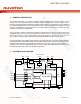
NAU7802 24-bit ADC 9.4 16-pin application circuit The built-in voltage regulator and built-in oscillator enable very low parts count applications as shown here. The signal input filter is optional, depending on the application requirements and can be expanded with decoupling capacitors to ground if needed. With a lithium-ion battery, an external voltage regulator for the DVDD supply may also be optional. Battery Charge Circuit 0.1uF 47 0.
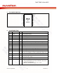
NAU7802 24-bit ADC 10 SUMMARY DEVICE REGISTER MAP Address Name Bit7 Bit6 Bit5 Bit4 Bit3 Bit2 Bit1 Bit0 Default 0x00 PU_CTRL AVDDS OSCS CR 0x01 CTRL1 CRP 0x02 CTRL2 CHS 0x03 OCAL1_B2 CH1 OFFSET Calibration[23:16] 0x00 0x04 OCAL1_B1 CH1 OFFSET Calibration[15:8] 0x00 0x05 OCAL1_B0 CH1 OFFSET Calibration[7:0] 0x00 0x06 GCAL1_B3 CH1 GAIN Calibration[31:24] 0x00 0x07 GCAL1_B2 CH1 GAIN Calibration[23:16] 0x80 0x08 GCAL1_B1 CH1 GAIN Calibration[15:8] 0x00 0x09 GCAL1_B0 CH1 GAIN Ca
NAU7802 24-bit ADC 11 DEVICE REGISTER MAP DETAILS 11.
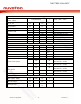
NAU7802 24-bit ADC 11.2 REG0x01:CTRL1 Register Default= 0x00 Bit Name Description Conversion Ready Pin Polarity (16 Pin Package Only) 1=CRDY pin is LOW Active (Ready when 0) 0=CRDY pin is High Active(Ready when 1) (default) Select the function of DRDY pin 1: DRDY output the Buffered Crystal Clock if OSCS=1 6 DRDY_SEL output the internal OSC clock if OSCS= 0 0: DRDY output the conversion ready (default) LDO Voltage 111 = 2.4 110 = 2.7 101 = 3.0 5:3 VLDO 100 = 3.3 011 = 3.6 010 = 3.9 001 = 4.2 000 = 4.
NAU7802 24-bit ADC 11.3 REG0x02:CTRL2 Register Default =0x00 Bit Name Description Analog input channel select 1 = Ch2 0 = Ch1 (default) Conversion rate select 111 = 320SPS 011 = 80SPS 6:4 CRS 010 = 40SPS 001 = 20SPS 000 = 10SPS (default) Read Only calibration result 3 CAL_ERR 1: there is error in this calibration 0: there is no error Write 1 to this bit will trigger calibration based on the selection in CALMOD[1:0] This is an "Action" register bit.
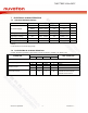
NAU7802 24-bit ADC 11.4 REG0x03-REG0x05: Channel 1 OFFSET Calibration offset register bit 23 22 21 20 19 18 17 16 15 14 13 12 11 10 9 8 7 6 5 4 3 2 1 - - - - - - - - - 0 - offset +/- 2-1 2-2 2-3 2-4 2-5 2-6 2-7 2-8 2-9 2-10 2-11 2-12 2-13 2 2 2 2 2 2 2 2 2 2 default 0 0 0 0 0 0 0 0 0 0 0 0 0 0 0 0 0 0 0 0 0 0 0 0 14 15 16 17 18 19 20 21 22 23 11.
NAU7802 24-bit ADC 11.
NAU7802 24-bit ADC 11.9 REG0x12-REG0x14: ADC Conversion Result REG0x12 (Read Only) ADCO_B2 ADC Conversion Result bit 23 to bit 16 REG0x13 (Read Only) ADCO_B1 ADC Conversion Result bit 15 to bit 8 REG0x14 (Read Only) ADCO_B0 ADC Conversion Result bit 7 to bit 0 Before reading an ADC Conversion Result, check if REG0x00 bit 5 CR=1 or DRDY pin showing Data Ready first. If not showing Data Ready, but a read of REG0x12 is performed, it will latch and shift out the previous conversion result.
NAU7802 24-bit ADC 11.10 REG0x15: ADC registers Bit Name Description Select the CLK_CHP clock frequency. REG_CPHS[1] REG_CPHS[0] CLK_CHP clock frequency 5:4 REG_CHPS 0 0 Reserved 0 1 Reserved 1 0 Reserved 1 1 turned off, high ('1') state Select the ADC input common mode for unipolar configuration. ADC_VCM[1] ADC_VCM[0] CHP_CLKSD Delay 3:2 ADC_VCM 0 0 disable 0 1 disable 0 Enable extended common mode. When voltage range close to REFN with ADC gain divided by 2.
NAU7802 24-bit ADC REG0x15-REG0x17: OTP Read Value and REG0x15 ADC Registers Read ADC registers and OTP[32:24] are sharing REG0x15 when read back, the REG0x1B[7] RD_OTP_SEL (default 0) is used as read select REG0x15 Read REG0x1B[7]=RD_OTP_SEL=1 Read back OTP[32:24] REG0x15 Read REG0x1B[7]=RD_OTP_SEL=0(default) Read back ADC Registers(default) REG0x16 Read Read back OTP[23:16] REG0x17 Read Read back OTP[15:8] 11.11REG0x18: Read Only 11.12REG0x19: Read Only 11.13REG0x1A: Read Only 11.
NAU7802 24-bit ADC 11.
NAU7802 24-bit ADC 12 PACKAGE DIMENSIONS 12.1 16L SOP – 150 mil Nuvoton Confidential - 38 - Revision 1.
NAU7802 24-bit ADC 12.2 PDIP16L - 300 mil A Nuvoton Confidential - 39 - Revision 1.
NAU7802 24-bit ADC 13 PART ORDERING INFORMATION Nuvoton Part Number Description NAU7802-SGI Package Material: G = Pb-free Package Package Style: S = SOP K = PDIP Package Type: 2 = Two channel 16-Pin Package Nuvoton Confidential - 40 - Revision 1.
NAU7802 24-bit ADC 14 REVISION HISTORY VERSION V0.9 V099a V 1.
NAU7802 24-bit ADC Important Notice Nuvoton Products are neither intended nor warranted for usage in systems or equipment, any malfunction or failure of which may cause loss of human life, bodily injury or severe property damage. Such applications are deemed, “Insecure Usage”.