
Data Sheet

ams Datasheet Page 7
[v1-04] 2018-Jul-09 Document Feedback
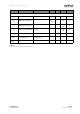
AS7265x − Absolute Maximum Ratings
Stresses beyond those listed under Absolute Maximum Ratings
of AS7265x may cause permanent damage to the device. These
are stress ratings only. Functional operation of the device at
these or any other conditions beyond those indicated under
Electrical Characteristics is not implied. Exposure to absolute
maximum rating conditions for extended periods may affect
device reliability. The device is not designed for high energy UV
(ultraviolet) environments, including upward looking outdoor
applications, which could affect long term optical performance.
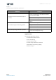
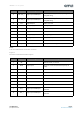
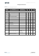
Figure 6:
Absolute Maximum Ratings of AS7265x
Symbol Parameter Min Max Unit Comments
Electrical Parameters
V
DD1_MAX
Supply Voltage VDD1 -0.3 5 V Pin VDD1 to GND
V
DD2_MAX
Supply Voltage VDD2 -0.3 5 V Pin VDD2 to GND
V
DD_IO
Input/Output Pin Voltage -0.3 VDD+0.3 V Input/Output Pin to GND
I
SCR
Input Current (latch-up
immunity)
± 100 mA JESD78D
Electrostatic Discharge
ESD
HBM
Electrostatic Discharge HBM ±1000 V JS-001-2014
ESD
CDM
Electrostatic Discharge CDM ±500 V JESD22-C101F
Temperature Ranges and Storage Conditions
T
STRG
Storage Temperature Range -40 85 °C
T
BODY
Package Body Temperature 260 °C
IPC/JEDEC J-STD-020. The
reflow peak soldering
temperature (body
temperature) is specified
according IPC/JEDEC
J-STD-020 “Moisture/Reflow
Sensitivity Classification for
Non-hermetic Solid State
Surface Mount Devices”
RH
NC
Relative Humidity
(non-condensing)
585%
MSL Moisture Sensitivity Level 3
Represents a 168 hour max.
floor lifetime
Absolute Maximum Ratings