
Data Sheet

Page 50 ams Datasheet
Document Feedback [v1-04] 2018-Jul-09
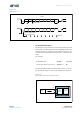
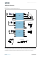
AS7265x − PCB Pad Layout
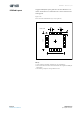
Suggested PCB pad layout guidelines for the LGA device are
shown. Flash Gold is recommended as a surface finish for the
landing pads.
Figure 62:
Recommended PCB Pad Layout (Top View)
Note(s):
1. Unless otherwise specified, all dimensions are in millimeters.
2. Add 0.05mm all around the nominal lead width and length for the PCB pad
land pattern.
3. This drawing is subject to change without notice.
PCB Pad Layout
4.05
3.85
Unit: mm
1
5
0.55
0.400.65