
Data Sheet

Page 4 ams Datasheet
Document Feedback [v1-04] 2018-Jul-09
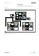
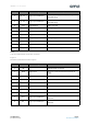
AS7265x − Pin Assignments
The device pin assignments are described below.
Figure 3:
Pin Diagram of AS7265x (Top View)
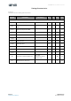
Figure 4:
AS72651 Pin Description
Pin No. Pin Name Pin Type Description
1 SLV1_RESN Digital Input and Output Reset pin for Slave 1 e.g. AS72652, active low
2 RESN Digital Input
Reset pin, active low (with internal pull-up to
VDD)
3 SCK Digital Output SPI serial clock
4 MOSI Digital Input and Output SPI MOSI
5 MISO Digital Input and Output SPI MISO
6 CSN Digital Output Chip select for external flash
7 NC Not functional, no connect
8 I2C_ENB Digital Input Selects UART (low) or I²C (high) operation
9 SCL_M Digital Output
I²C master clock for communication with
AS72652 and AS72653
10 SDA_M Digital Input and Output
I²C master data for communication with AS72652
and AS72653
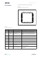
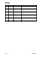
Pin Assignments
1
5
610
11
15
1620