
Data Sheet

ams Datasheet Page 23
[v1-04] 2018-Jul-09 Document Feedback
AS7265x − Detailed Description
If BANK is set in the AS72651 to Mode 0 or Mode 1, data is ready
after the 1
st
integration time. If BANK is set to Mode 2, data is
ready after two integration times.
For interrupt operation using I²C registers, if interrupts are en-
abled and data is ready, the INT pin is set low and DATA_RDY is
set to 1. Reading the raw or calibration data releases (returns
high) the interrupt. For multi-byte sensor data (2 or 4 bytes),
after the 1st byte is read the remaining bytes are shadow pro-
tected in case an integration cycle completes just after the 1st
byte is read. The sensors continue to gather information at the
rate of the integration time, hence if the sensor registers are not
read when the interrupt line goes low, it will stay low and the
next cycle’s sensor data will be available in the registers at the
end of the next integration cycle.
For interrupt operation using AT Commands, if interrupts are
enabled and data is ready the INT pin is set low and is released
(returns high) after any sensor data is read.
Required Flash Memory
Serial flash is a required operating companion for this device,
and enables the I²C and UART interfaces, as well as enabling
calibrated data results. Supported device types are noted in
Ordering & Contact Information at the end of this document.
Required operating code can be downloaded at
download.ams.com.
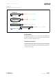
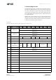
I²C Slave Interface
If selected by the I2C_ENB pin setting, interface and control can
be accomplished through an I²C compatible slave interface to
a set of registers that provide access to device control functions
and output data. These registers on the AS72651 are, in reality,
implemented as virtual registers in software. The actual I²C slave
hardware registers number only three and are described in the
table below. The steps necessary to access the virtual registers
defined in the following are explained in pseudocode for exter-
nal I²C master writes and reads below.
I²C Feature List
• Fast mode (400kHz).
• 7+1-bit addressing mode.
• Write format: Byte.
• Read format: Byte.
• SDA input delay and SCL spike filtering by integrated
RC-components.