AS7265x Smart 18-Channel VIS to NIR Spectral_ ID 3-Sensor Chipset with Electronic Shutter General Description The AS7265x chipset consists of three sensor devices AS72651 with master capability, AS72652 and AS72653. The multispectral sensors can be used for spectral identification in a range from visible to NIR. Every of the three sensor devices has 6 independent on-device optical filters whose spectral response is defined in a range from 410nm to 940nm with FWHM of 20nm.
AS7265x − General Description Figure 1: AS7265x Chip-Set Benefits and Features Benefits Features • 3 chip set including master device delivering 18 visible and NIR channels from 410nm to 940nm each with 20nm FWHM • Compact 18-channel spectrometry chip-set solution • UART or I²C slave digital Interface • Visible filter set realized by silicon interference filters • 16-bit ADC with digital access • No additional signal conditioning required • Programmable LED drivers • 2.7V to 3.
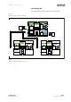
AS7265x − General Description Block Diagram The functional blocks of this device are shown below: Figure 2: AS7265x Chip-Set Block Diagram VDD2 VDD1 AS72651 Communication Spectral_ID Sensor VDD VDD LED Drivers LED_IND I2C_ENB Micro Controller Unit (MCU) RX / SCL_S TX / SDA_S UART or I2C Slave INT Current Control R S T U V W VDD Firmware Interface SDA_M SCL_M LED_DRV I2C Master VDD °C MISO OSC 16MHz SLV1_RESN SLV2_RESN RESN SPI Master Serial Flash Memory MOSI SCK CSN GND VDD
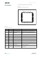
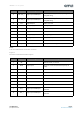
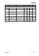
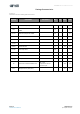
AS7265x − Pin Assignments Pin Assignments The device pin assignments are described below. Figure 3: Pin Diagram of AS7265x (Top View) 20 16 1 15 5 11 6 10 Figure 4: AS72651 Pin Description Pin No. Pin Name 1 SLV1_RESN 2 Pin Type Description Digital Input and Output Reset pin for Slave 1 e.g.
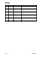
AS7265x − Pin Assignments Pin No.
AS7265x − Pin Assignments Pin No.
AS7265x − Absolute Maximum Ratings Absolute Maximum Ratings Stresses beyond those listed under Absolute Maximum Ratings of AS7265x may cause permanent damage to the device. These are stress ratings only. Functional operation of the device at these or any other conditions beyond those indicated under Electrical Characteristics is not implied. Exposure to absolute maximum rating conditions for extended periods may affect device reliability.
AS7265x − Electrical Characteristics Electrical Characteristics All limits are guaranteed with VDD = VDD1 = VDD2 = 3.3V, T AMB = 25°C. The parameters with min and max values are guaranteed with production tests or SQC (Statistical Quality Control) methods. VDD1 and VDD2 should be sourced from the same power supply output.
AS7265x − Electrical Characteristics Symbol Parameter Conditions Min Typ Max Unit -1 1 μA Digital Inputs and Outputs IIH, IIL Logic Input Current Vin=0V or VDD VIH CMOS Logic High Input 0.7* VDD VDD V VIL CMOS Logic Low Input 0 0.3* VDD V VOH CMOS Logic High Output I=1mA VDD0.4 V VOL CMOS Logic Low Output I=1mA 0.4 V tRISE(1) Current Rise Time C(Pad)=30pF 5 ns tFALL(1) Current Fall Time C(Pad)=30pF 5 ns Note(s): 1. Guaranteed by design, not tested in production.
AS7265x − Electrical Characteristics Timing Characteristics Figure 8: AS7265x I²C Slave Timing Characteristics Symbol Parameter Conditions Min Typ Max Unit 400 kHz I²C Interface fSCLK SCL Clock Frequency tBUF Bus Free Time Between a STOP and START 1.3 μs Hold Time (Repeated) START 0.6 μs tLOW LOW Period of SCL Clock 1.3 μs tHIGH HIGH Period of SCL Clock 0.6 μs tSU:STA Setup Time for a Repeated START 0.
AS7265x − Electrical Characteristics Figure 9: I²C Slave Timing Diagram tR tF tLOW SCL P tHIGH S tHD:STA S tSU:DAT tHD:DAT P t SU:STA tSU:STO VIH SDA tBUF Stop VIL Start Figure 10: AS72651 SPI Timing Characteristics Symbol Parameter Conditions Min Typ Max Unit 16 MHz SPI Interface fSCK Clock Frequency 0 tSCK_H Clock High Time 40 ns tSCK_L Clock Low Time 40 ns tSCK_RISE SCK Rise Time 5 ns tSCK_FALL SCK Fall Time 5 ns tCSN_S CSN Setup Time Time between CSN high-
AS7265x − Electrical Characteristics Figure 11: SPI Master Write Timing Diagram t CS N_DIS CSN tSCK_RISE tCSN_S tCSN_H tSCK_FALL SCK t DO_S MOSI tDO_H MSB LSB HI-Z HI-Z MISO Figure 12: SPI Master Read Timing Diagram CSN_xx tSCK_H tSCK_L SCK tDI_V Dont care MOSI MISO Page 12 Document Feedback MSB LSB ams Datasheet [v1-04] 2018-Jul-09
AS7265x − Typical Operating Characteristics Typical Operating Characteristics Optical Characteristics All optical characteristics are optimized for diffused light. When using a point light source or collimated light on the sensor, the sensor opening must be covered by a lambertian diffuser with achromatic characteristics. Diffusor of Tsujiden like D121UP have been successfully tested at ams. If in the application diffused light, e.g. used by a reflective surface, no additional diffuser is required.
AS7265x − Typical Operating Characteristics Figure 15: AS72651 Spectral Responsivity AS72651, 6-Channel Spectral Response 1.2 R 610 S 680 T U 730 760 V 810 W 860 Normalized Responsivity 1 0.8 0.6 0.4 0.
AS7265x − Typical Operating Characteristics Symbol Parameter dark Dark Channel Counts AFOV Average Field of View Test Conditions Channel (nm) Min Typ Max Unit 5 counts GAIN=64, TAMB=25°C tint=165ms ±20.5 deg Note(s): 1. Calibration and measurements are made using diffused light. 2. Each channel is tested with GAIN = 16x, Integration Time (INT_T) = 166ms and VDD = VDD1 = VDD2 = 3.3V, TAMB =25°C. 3. The accuracy of the channel counts/μW/cm 2 is ±12%. 4.
AS7265x − Typical Operating Characteristics Figure 18: Optical Characteristics of AS72652 (Pass Band) (1) Symbol Parameter Conditions Channel (nm) Min Typ Max Unit G Channel G 3300K White LED(2) 560 35(3) counts/ (μW/cm2) H Channel H 3300K White LED(2) 585 35(3) counts/ (μW/cm2) I Channel I 3300K White LED(2) 645 35(3) counts/ (μW/cm2) J Channel J 3300K White LED(2) 705 35(3) counts/ (μW/cm2) K Channel K Incandescent(2) 900 35(3) counts/ (μW/cm2) L Channel L 940nm L
AS7265x − Typical Operating Characteristics Figure 19: AS72653 Spectral Responsivity AS72653, 6-Channel Spectral Response (w/AS72651 as controller) Normalized Responsivity 1.2 D E B C F A 410 435 460 485 510 535 1 0.8 0.6 0.4 0.
AS7265x − Typical Operating Characteristics Figure 20: Optical Characteristics of AS72653 (Pass Band)(1) Conditions Channel (nm) Symbol Parameter A Channel A 410 35(3) counts/ (μW/cm2) B Channel B 435 35(3) counts/ (μW/cm2) C Channel C 460 35(3) counts/ (μW/cm2) D Channel D 485 35(3) counts/ (μW/cm2) E Channel E 510 35(3) counts/ (μW/cm2) F Channel F 535 35(3) counts/ (μW/cm2) FWHM Full Width Half Max 20 nm Wacc Wavelength Accuracy dark Dark Channel Counts AFOV A
AS7265x − Detailed Description Detailed Description AS7265x 18-Channel Spectral_ID Detector Overview Each of the three AS7265x Spectral_ID devices are next-generation digital 6-channel spectral sensor devices. Each of the 6 channels has a Gaussian filter characteristic with a full width half maximum (FWHM) bandwidth of 20nm. The filters use an interference topology design providing high stability in terms of drift in time and temperature. The drifts are so small that it is undetectable in the measurement.
AS7265x − Detailed Description This spectral data conversion process operates continuously, new data is available after each IT ms period.
AS7265x − Detailed Description Figure 22: Bank Mode and Data Conversion BANK Mode 0 One Conversion S, T, U, V, I, G, H, K, C, A, B, E Integration Time BANK Mode 1 One Conversion R, T, U, W, L, G, H, J, F, A, B, D Integration Time BANK Mode 2 1st Conversion S, T, U, V, I, G, H, K, C, A, B, E 2nd Conversion Integration Time R, T, U, W, L, G, H, J, F, A, B, D Integration Time RC Oscillator The timing generation circuit consists of on-chip 16MHz, temperature compensated oscillators, which provide the
AS7265x − Detailed Description Reset Pulling down the RESN pin for longer than 100ms resets the AS72651 which proceed to reset the AS72562 and the same RESN signal shown below can be used directly to reset the AS72653. Figure 23: Reset Circuit VDD Spectral_ID Engine Reset AS72651 RESN Push > 100ms AS7265x LED_IND Controls There are LED_IND pins on all AS7265x devices.
AS7265x − Detailed Description If BANK is set in the AS72651 to Mode 0 or Mode 1, data is ready after the 1 st integration time. If BANK is set to Mode 2, data is ready after two integration times. For interrupt operation using I²C registers, if interrupts are enabled and data is ready, the INT pin is set low and DATA_RDY is set to 1. Reading the raw or calibration data releases (returns high) the interrupt.
AS7265x − Detailed Description Figure 24: I²C Slave Device Address and Physical Registers Entity Description Note 8-bit slave address Byte = 1001001x (device address = 49 hex) • x= 1 for Master Read (byte = 93 hex) • x= 0 for Master Write (byte = 92 hex) I²C slave interface STATUS register. Read-only. Register Address = 0x00 Bit 1: TX_VALID • 0 - New data may be written to WRITE register • 1 -WRITE register occupied. Do NOT write. Bit 0: RX_VALID • 0 -No data is ready to be read in READ register.
AS7265x − Detailed Description I²C Virtual Register Byte Write Pseudocode Poll I²C slave STATUS register; If TX_VALID bit is 0, a write can be performed on the interface; Send a virtual register address and set the MSB of the register address to 1 to indicate the pending write; Poll I²C slave STATUS register; If TX_VALID bit is 0, the virtual register address for the write has been received and the data may now be written; Write the data.
AS7265x − Detailed Description I²C Virtual Register Byte Read, detailed below, shows the pseudocode necessary to read virtual registers on the AS72651. Note that in this case, reading a virtual register, the register address is not modified.
AS7265x − Detailed Description 4-Byte Floating-Point (FP) Registers Several 4 byte registers (hex) are used by the AS72651. Here is an example of how these registers are used to represent floating point data (based on the IEEE 754 standard).
AS7265x − Detailed Description I²C Virtual Register Set The figure below provides a summary of the AS72651 I²C register set for the AS72651 which serves as the master interface of the 3 device AS7265x set. Figures after that provide additional register details. All register data is hex, and all multi-byte entities are Big Endian (most significant byte is situated at the lowest register address).
AS7265x − Detailed Description Addr Name 0x14 Calibrated value channel R, G, A CAL CHAN0_0 0x15 Calibrated value channel R, G, A CAL CHAN0_1 0x16 Calibrated value channel R, G, A CAL CHAN0_2 0x17 Calibrated value channel R, G, A CAL CHAN0_3 0x18 Calibrated value channel S, H, B CAL CHAN0_0 0x19 Calibrated value channel S, H, B CAL CHAN0_1 0x1A Calibrated value channel S, H, B CAL CHAN0_2 0x1B Calibrated value channel S, H, B CAL CHAN0_3 0x1C Calibrated value channel T, I, C CAL
AS7265x − Detailed Description Addr Name 0x27 Calibrated value channel V, K, E CAL CHAN0_3 0x28 Calibrated value channel W, L, F CAL CHAN0_0 0x29 Calibrated value channel W, L, F CAL CHAN0_1 0x2A Calibrated value channel W, L, F CAL CHAN0_2 0x2B Calibrated value channel W, L, F CAL CHAN0_3 0x48 FW control 0x49 FW byte count FW_BYTE_COUNT_H 0x4A FW byte count FW_BYTE_COUNT_L 0x4B FW payload HW version H 0x4F DEV SEL 0x50 COEF DATA COEF_DATA_0 0x51 COEF DATA COEF_DATA_1 0x
AS7265x − Detailed Description Detailed Register Descriptions Figure 27: HW Version Registers Addr: 0x00,0x01 HW Version Bit Bit Name Default Access Bit Description 15:8 HW version H 0x40 R Device type 7:0 HW version L 0x41 R HW version Figure 28: FW Version Registers Addr: 0x02,0x03 FW Version Bit Bit Name Default Access 15:8 FW version H 0 R/W 7:0 FW version L 0 R/W Bit Description Set register 0x02, 0x03 to 0x01 to 0x03 to get each firmware positions high byte 0x01: MAJO
AS7265x − Detailed Description The maximum sensitivity value depends on the integration time. For every 2.78ms of integration time, the maximum sensitivity value increases by 1024 counts. This means that to be able to reach the full sensitivity scale, the sensitivity has to be at least 64*2.78ms. Figure 30: Integration Time Register Addr: 0x05 Bit Bit Name Integration Time Default Access Bit Description Integration time = * 2.
AS7265x − Detailed Description Figure 32: LED Configuration Register Addr: 0x07 LED Configuration Bit Bit Name Default Access Bit Description 7 READ_ERR 0 R 5:4 LED_DRV 00 R/W LED_DRV current limit: b00=12.
AS7265x − Detailed Description Figure 35: RAW Value Channel T,I,C Register Addr: 0x0C/0x0D RAW Value Channel T,I,C Bit Bit Name Default Access 15:8 RAW value H - R 7:0 Raw value L - R Bit Description Channel T or G or A depends on register DEV_ SEL Figure 36: RAW Value Channel U,J,D Register Addr: 0x0E,0x0F RAW Value Channel U,J,D Bit Bit Name Default Access 15:8 RAW value H - R 7:0 Raw value L - R Bit Description Channel U or H or B depends on register DEV_ SEL Figure 37: R
AS7265x − Detailed Description Figure 39: Calibrated Value Channel R,G,A Register Addr: 0x17,0x016,0x15,0x014 Calibrated Value Channel R,G,A Bit Bit Name Default Access 31:24 CAL CHAN0_3 FF R 23:16 CAL CHAN0_2 FF R 15:8 CAL CHAN0_1 FF R 7:0 CAL CHAN0_0 FF R Bit Description Channel R or J or D depends on register DEV_ SEL Figure 40: Calibrated Value Channel S, H, B Register Addr: 0x1B,0x01A,0x19,0x018 Calibrated Value Channel S,H,B Bit Bit Name Default Access 31:24 CAL CHAN1
AS7265x − Detailed Description Figure 42: Calibrated Value Channel U, J, D Register Addr: 0x23,0x022,0x21,0x20 Calibrated Value Channel U,J,D Bit Bit Name Default Access 31:24 CAL CHAN3_3 FF R 23:16 CAL CHAN3_2 FF R 15:8 CAL CHAN3_1 FF R 7:0 CAL CHAN3_0 FF R Bit Description Channel U or H or B depends on register DEV_ SEL Figure 43: Calibrated Value Channel V, K, E Register Addr: 0x27,0x026,0x25,0x24 Calibrated Value Channel V,K,E Bit Bit Name Default Access 31:24 CAL CHAN4
AS7265x − Detailed Description Figure 45: FW Control Register Addr: 0x48 FW Control Bit Bit Name Default Access Bit Description 7 START R/W 6 STOP W Reset firmware update state machine 5 BYTES_ TRANSFERRED R All 56kbytes are transferred 4 LOCK R/W 3 SWITCH W Switch between both firmware 2 BANK1 R Set if bank 1 is active, else bank 2 1 ERROR R Error occurred while firmware update 0 CHKSUM R Checksum of other bank is valid Set bit once to configure the device update Loc
AS7265x − Detailed Description Figure 48: DEV SEL Register Addr: 0x4F DEV SEL Bit Bit Name Default Access Bit Description 5 SECOND SLAVE 0 R Second slave Available 5 FIRST SLAVE 0 R First slave available 1:0 SELECT DATA 00 R/W 0x00: Select master data 0x01: Select first slave data 0x02: Select second slave data Figure 49: COEF DATA Register Addr: 0x53,0x52,0x51,0x50 COEF DATA Bit Bit Name Default Access 31:24 COEF_DATA_ 3 R/W 23:16 COEF_DATA_ 2 R/W 15:8 COEF_DATA_ 1 R/
AS7265x − Detailed Description Figure 51: COEF WRITE Register Addr:0x55 Bit Bit Name 7:0 COEF_WRITE COEF WRITE Default Access R/W Bit Description Set sub addresses to write different calibration data from COEF_DATA register to persistent memory AS72651 I 2 C Firmware (FW) Update Procedure • In the FW Update Control register set the Start_XFR bit to 1.
AS7265x − Detailed Description Figure 53: Firmware Byte Count, High Byte Register Addr: 0x61/0xE1 Bit Bit Name 7:0 FWBC_HIGH Firmware Byte Count, High Byte Default Access Bit Description R Firmware byte address to be downloaded next, High Byte Figure 54: Firmware Byte Count, Low Byte Register Addr: 0x62/0xE2 Bit Bit Name 7:0 FWBC_LOW Firmware Byte Count, Low Byte Default Access R Bit Description Firmware byte address to be downloaded next, Low Byte Figure 55: Firmware Download Register A
AS7265x − Detailed Description UART Command Interface If selected by the I2C_ENB pin setting, the UART module implements the TX and RX signals as defined in the RS-232 / V.24 standard communication protocol. Serial flash EPROM is a required operating companion device to enable the UART command interface.
AS7265x − Detailed Description Figure 57: UART Protocol Data Bits TX D0 D1 Start Bit D2 D3 D4 D5 D6 D7 Stop Bit Tbit=1/Baude Rate Always Low RX D0 Next Start Always High D0 D1 D2 D3 D4 D5 D6 D7 D0 Start Bit detected After Tbit/2: Sampling of Start Bit After Tbit: Sampling of Data Sample Points AT Command Interface The microprocessor interface to control the AS72651 Spectral_ ID sensor(s) is via AT Commands across the UART interface.
AS7265x − Detailed Description In the AT Commands figure below, numeric values may be specified with no leading prefix, in which case they will be interpreted as decimals, or with a leading “0x” to indicate that they are hexadecimal numbers. The commands are loosely grouped into functional areas. Texts appearing between angle brackets (‘<‘and ‘>‘) are commands or response arguments. A carriage return character, a linefeed character, or both may terminate commands and responses.
AS7265x − Detailed Description Commands Direction Description Format Value Range Default Control ATINTTIME R/W Set sensor integration time. Integration time = * ~2.8ms. ATGAIN R/W Set sensor gain: 0=1x gain, 1=3.
AS7265x − Detailed Description Commands ATBURST Direction R/W Description Format Value Range Default Sends a number of calibrated data without separate requests second parameter for the burst mode is optionally format: Send: ATBURST=10,0 or ATBURST=10 Read: ATBURST ≥ 10,0 OK DEC BURST NUMBER: 0 - Burst mode is deactivated 1-254 - Number of burst transfers 255 - Send unlimited bursts (stops with ATBURST=0) 0 BURST MODE: 0 - Raw values (default, like ATDATA) 1 - Calibrated values (like ATCDATA)
AS7265x − Detailed Description Commands Format Value Range Default HEX [1...0] LED_IND: b00=1mA; b01=2mA; b10=4mA; b11=8mA [5...4] LED_DRV: b00=12.5mA; b01=25mA; b10=50mA; b11=100mA 0x00 R/W Sets LED_IND and LED_DRV current for second I2C slave HEX [1...0] LED_IND: b00=1mA; b01=2mA; b10=4mA; b11=8mA [5...4] LED_DRV: b00=12.5mA; b01=25mA; b10=50mA; b11=100mA 0x00 ATFRST W Factory Reset. Stored values are reset to ‘Factory’ defaults. Afterwards a software reset is started.
AS7265x − Detailed Description Commands ATFWS ATFWL ATFWC ATFWA ams Datasheet [v1-04] 2018-Jul-09 Direction Description Format Value Range Default W Tests the checksum on the non-active FW partition and, if correct, switches active partition. This is a toggle and used to toggle between the 2 FW partitions. Note: The first 5 bytes in page 0 are not touched.
AS7265x − Application Information Application Information Figure 60: Typical AS7265x 18-Channel Application Circuit 3V3 U3 +5V 3V3 D9 LED 17 C7 100nF C8 1u0 14 RESN TP9 R10 10k GND 2 RESN 16 R11 200R D11 3V3 CSN VDD2 MISO RESN MOSI GND SCK AS72651 GND LED_651 15 LED_IND 18 I2C_ENB LED_DRV LED_IND NC GRN SLV2_RESN ---> COMM_RX 11 <--- COMM_TX 12 INT 13 TP10 INT SLV1_RESN RX/SCL_S TX/SDA_S SDA_M INT SCL_M 3V3 C10 D12 100nF LED R17 10k 6 CSN_EE 5 SPI_MISO 4
AS7265x − Package Drawings & Markings Package Drawings & Markings Figure 61: Package Drawing RoHS Green Note(s): 1. All dimensions are in millimeters. 2. XXXXX = tracecode. 3. Unless otherwise specified tolerances are: Angular (±.5°), Two Place Decimal (±.1), Three Place Decimal (±.05). 4. Contact finish is Au. 5. This package contains no lead (Pb). 6. This drawing is subject to change without notice.
AS7265x − PCB Pad Layout PCB Pad Layout Suggested PCB pad layout guidelines for the LGA device are shown. Flash Gold is recommended as a surface finish for the landing pads. Figure 62: Recommended PCB Pad Layout (Top View) 0.65 0.40 Unit: mm 0.55 3.85 1 5 4.05 Note(s): 1. Unless otherwise specified, all dimensions are in millimeters. 2. Add 0.05mm all around the nominal lead width and length for the PCB pad land pattern. 3. This drawing is subject to change without notice.
AS7265x − PCB Pad Layout In order to prevent interference, avoid trace routing feedthroughs with exposure directly under the AS7265x devices. An example routing is illustrated in the Figure 63.
AS7265x − Mechanical Data Mechanical Data Figure 64: Tape & Reel Information Note(s): 1. All dimensions in millimeters unless of otherwise stated. 2. Measured from centreline of sprocket hole to centreline of pocket. 3. Cumulative tolerance of 10 sprocket holes is ±0.20. 4. Measured from centreline of sprocket hole to centreline of pocket. 5. Other material available.
AS7265x − Soldering & Storage Information Soldering & Storage Information Soldering Information The module has been tested and has demonstrated an ability to be reflow soldered to a PCB substrate. The solder reflow profile describes the expected maximum heat exposure of components during the solder reflow process of product on a PCB. Temperature is measured on top of component. The components should be limited to a maximum of three passes through this solder reflow profile.
AS7265x − Soldering & Storage Information Manufacturing Process Considerations The AS72651,AS72652 and AS72653 packages are compatible with standard reflow no-clean and cleaning processes including aqueous, solvent or ultrasonic techniques. However, as an open-aperture device, precautions must be taken to avoid particulate or solvent contamination as a result of any manufacturing processes, including pick and place, reflow, cleaning, integration assembly and/or testing.
AS7265x − Soldering & Storage Information Floor Life The module has been assigned a moisture sensitivity level of MSL 3.
AS7265x − Ordering & Contact Information Ordering & Contact Information Figure 67: Ordering Information Ordering Code Package Marking Description Delivery Form Delivery Quantity Tape & Reel 2000 pcs/reel AS72651-BLGT 20-pin LGA AS7265 Smart 6-Channel NIR Spectral_ID Sensor with Electronic Shutter and 18-Channel AS7265x Master Capability AS72652-BLGT 20-pin LGA AS7266 Smart 6-Channel NIR Spectral_ID Sensor with Electronic Shutter Tape & Reel 2000 pcs/reel AS72653-BLGT 20-pin LGA AS7267
AS7265x − RoHS Compliant & ams Green Statement RoHS Compliant & ams Green Statement RoHS: The term RoHS compliant means that ams AG products fully comply with current RoHS directives. Our semiconductor products do not contain any chemicals for all 6 substance categories, including the requirement that lead not exceed 0.1% by weight in homogeneous materials. Where designed to be soldered at high temperatures, RoHS compliant products are suitable for use in specified lead-free processes.
AS7265x − Copyrights & Disclaimer Copyrights & Disclaimer Copyright ams AG, Tobelbader Strasse 30, 8141 Premstaetten, Austria-Europe. Trademarks Registered. All rights reserved. The material herein may not be reproduced, adapted, merged, translated, stored, or used without the prior written consent of the copyright owner. Devices sold by ams AG are covered by the warranty and patent indemnification provisions appearing in its General Terms of Trade.
AS7265x − Document Status Document Status Document Status Product Preview Preliminary Datasheet Datasheet Datasheet (discontinued) ams Datasheet [v1-04] 2018-Jul-09 Product Status Definition Pre-Development Information in this datasheet is based on product ideas in the planning phase of development.
AS7265x − Revision Information Revision Information Changes from 1-03 (2017-Oct-17) to current revision 1-04 (2018-Jul-09) Page Updated text under General Description 1 Updated text under Key Benefits & Features 1 Updated Figure 2 (AS7265x Chip- Set Block Diagram) 3 Renamed Figure 3 to “Pin Diagram of AS72651,AS72652 and AS72653 (Top View)” 4 Updated Figure 4 (AS72651 pin description) 4 Added Figure 5 (AS72652 and AS72653 pin description) 5 Updated text under “Absolute Maximum Ratings” (repl
AS7265x − Revision Information Changes from 1-03 (2017-Oct-17) to current revision 1-04 (2018-Jul-09) Page Updated Figure 59 (AS7265x AT Commands) and text above it 43 Updated Figure 60 (Typical AS7265x 18-Channel Application Circuit) 48 Updated text under Manufacturing Process Considerations (replaced AS72651 with AS72651, AS72652,AS72653) 54 Updated note under Figure 67 56 Note(s): 1.
AS7265x − Content Guide Content Guide 1 1 2 3 General Description Key Benefits & Features Applications Block Diagram 4 7 Pin Assignments Absolute Maximum Ratings 8 10 Electrical Characteristics Timing Characteristics 13 13 Typical Operating Characteristics Optical Characteristics 19 19 22 23 23 23 24 25 26 27 28 31 39 41 41 41 41 41 42 Detailed Description AS7265x 18-Channel Spectral_ID Detector Overview Channel Data Conversion of the AS7265x Devices RC Oscillator Temperature Sensor Reset AS7265
AS7265x − Content Guide 56 57 58 59 60 ams Datasheet [v1-04] 2018-Jul-09 Ordering & Contact Information RoHS Compliant & ams Green Statement Copyrights & Disclaimer Document Status Revision Information Page 63 Document Feedback