
Data Sheet

DocID031281 Rev 2 5/35
VL53L1X Product overview
35
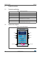
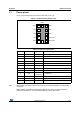
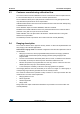
1.3 Device pinout
Figure 2 shows the pinout of the VL53L1X (see also Figure 18).
Figure 2. VL53L1X pinout (bottom view)
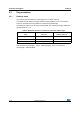
Note: AVSSVCSEL and GND are ground pins and can be connected together in the application
schematics.
GND2, GND3, and GND4 are standard pins that we force to the ground domain in the
application schematics to avoid possible instabilities if set to other states.
Table 2. VL53L1X pin description
Pin number Signal name Signal type Signal description
1 AVDDVCSEL Supply VCSEL supply, to be connected to main supply
2 AVSSVCSEL Ground VCSEL ground, to be connected to main ground
3 GND Ground To be connected to main ground
4 GND2 Ground To be connected to main ground
5 XSHUT Digital input Xshutdown pin, active low
6 GND3 Ground To be connected to main ground
7 GPIO1 Digital output Interrupt output. Open drain output
8 DNC Digital input Do not connect, must be left floating
9SDA
Digital
input/output
I
2
C serial data
10 SCL Digital input I
2
C serial clock input
11 AVDD Supply Supply, to be connected to main supply
12 GND4 Ground To be connected to main ground
$9''9&6(/
$9669&6(/
*1'
*1'
;6+87
$9''
6&/
6'$
'1&
*3,2
*1'
*1'