
Data Sheet

Electrical characteristics VL53L1X
24/35 DocID031281 Rev 2
5.4 Current consumption
5.5 Digital I/O electrical characteristics
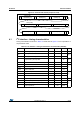
Table 16. Power consumption at ambient temperature
(1)
1. All current consumption values include silicon process variations. Temperature and voltage are nominal
conditions (23 °C and AVDD 2v8). All values include AVDD and AVDDVCSEL.
Parameter Min. Typ. Max. Unit
HW standby 3 5 7
uASW standby
(2)
2. In 2v8 (IOVDD) mode, pull ups have to be modified, then SW Standby consumption is increased by 0.6 µA.
469
Inter measurement 20
Ranging average (AVDD + AVDDVCSEL)
(3)
(4)
3. Average consumption during ranging operation in long distance mode.
4. Peak current (including VCSEL) can reach 40 mA.
16 18 mA
Average power consumption at 10 Hz with 33 ms
timing budget
20
mW
Average power consumption at 1 Hz with 20 ms
timing budget when no target detected
0.9
Average power consumption at 1 Hz with 20 ms
timing budget when target detected
1.4
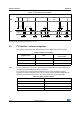
Table 17. Digital I/O electrical characteristics
Symbol Parameter Min. Typ. Max. Unit
Interrupt pin (GPIO1)
V
IL
Low level input voltage -
-
0.3 IOVDD
V
V
IH
High level input voltage 0.7 IOVDD -
V
OL
Low level output voltage
(I
OUT
= 4 mA)
-0.4
V
OH
High level output voltage
(I
OUT
= 4 mA)
IOVDD-0.4 -
F
GPIO
Operating frequency
(C
LOAD
= 20 pF)
0108MHz
I
2
C interface (SDA/SCL)
V
IL
Low level input voltage -0.5
-
0.6
V
V
IH
High level input voltage 1.12 IOVDD+0.5
V
OL
Low level output voltage
(I
OUT
= 4 mA)
-0.4
I
IL
/
IH
Leakage current
(1)
1. AVDD = 0 V
-10
µA
Leakage current
(2)
2. AVDD = 2.85 V; I/O voltage = 1.8 V
-0.15