
Data Sheet

Control interface VL53L1X
22/35 DocID031281 Rev 2
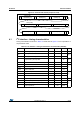
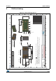
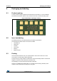
Figure 17. I
2
C timing characteristics
All timings are measured from either V
IL
or V
IH
.
4.2 I
2
C interface - reference registers
The registers shown in the table below can be used to validate the user I
2
C interface.
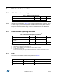
Note: The I
2
C read/writes can be 8,16 or 32-bit. Multi-byte reads/writes are always addressed in
ascending order with MSB first as shown in
Table 12.
The customer must use the VL53L1X software driver for easy and efficient ranging
operations to match performance and accuracy criteria. Hence full register details are not
exposed. The customer should refer to the VL53L1X API user manual (UM2356).
SDA
SCL
t
HD.STA
t
R
t
HIGH
t
F
t
SU.DAT
t
HD.DAT
t
SU.STA
t
SU.STO
...
...
t
HD.STA
t
LOW
t
BUF
stopstartstop start
V
IH
V
IL
V
IH
V
IL
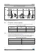
Table 11. Reference registers
Register name Index
After fresh reset, without
driver loaded
Model ID 0x010F 0xEA
Module Type 0x0110 0xCC
Mask Revision 0x0111 0x10
Table 12. 32-bit register example
Register address Byte
Address MSB
Address + 1 ..
Address + 2 ..
Address + 3 LSB