
Data Sheet
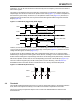

Electrode trace routing: Keep the electrode trace (and the electrode itself) away from other signal, power,
and ground traces including over or next to ground planes. Adjacent switching signals can induce noise
onto the sensing signal; any adjacent trace or ground plane next to, or under, the electrode trace will
cause an increase in Cx load and desensitize the device.
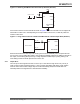
Note: For proper operation, a 100 nF (0.1 μF) ceramic bypass capacitor must be used directly between
Vdd and Vss to prevent latch-up if there are substantial Vdd transients; for example, during an ESD
event. The bypass capacitor should be placed very close to the Vss and Vdd pins.
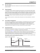
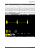
4.5 Power On
On initial power up, the QT1011 requires approximately 100 ms to power on to allow power supplies to
stabilize. During this time the OUT pin state is not valid and should be ignored.
AT42QT1011
© 2017 Microchip Technology Inc.
Datasheet
DS40001947A-page 16