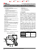
Sample & Buy Product Folder Support & Community Tools & Software Technical Documents bq24072, bq24073, bq24074, bq24075, bq24079 SLUS810K – SEPTEMBER 2008 – REVISED MARCH 2015 bq2407x 1.
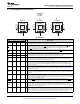
bq24072, bq24073, bq24074, bq24075, bq24079 SLUS810K – SEPTEMBER 2008 – REVISED MARCH 2015 www.ti.com Table of Contents 1 2 3 4 5 6 7 8 Features .................................................................. Applications ........................................................... Description ............................................................. Revision History..................................................... Description (continued).........................................
bq24072, bq24073, bq24074, bq24075, bq24079 www.ti.com SLUS810K – SEPTEMBER 2008 – REVISED MARCH 2015 Changes from Revision E (August 2010) to Revision F • Page Changed 10 x 45 s/kΩ to 10 x 48 s/kΩ under section Program 6.25hour......(TMR) ........................................................... 30 Changes from Revision D (June 2009) to Revision E Page • Changed globally RT1 and RT2 to Rs and Rp.......................................................................................................
bq24072, bq24073, bq24074, bq24075, bq24079 SLUS810K – SEPTEMBER 2008 – REVISED MARCH 2015 www.ti.com 5 Description (continued) Additionally, the regulated system input enables instant system turn-on when plugged in even with a totally discharged battery. The power-path management architecture also lets the battery supplement the system current requirements when the adapter cannot deliver the peak system currents, thus enabling the use of a smaller adapter.
bq24072, bq24073, bq24074, bq24075, bq24079 www.ti.
bq24072, bq24073, bq24074, bq24075, bq24079 SLUS810K – SEPTEMBER 2008 – REVISED MARCH 2015 www.ti.com Pin Functions (continued) PIN NAME I/O DESCRIPTION — – There is an internal electrical connection between the exposed thermal pad and the VSS pin of the device. The thermal pad must be connected to the same potential as the VSS pin on the printed circuit board. Do not use the thermal pad as the primary ground input for the device. VSS pin must be connected to ground at all times.
bq24072, bq24073, bq24074, bq24075, bq24079 www.ti.com SLUS810K – SEPTEMBER 2008 – REVISED MARCH 2015 8.3 Recommended Operating Conditions MIN MAX 4.35 26 ’72, ’73, ‘75, '79 4.35 6.4 ‘74 4.35 10.2 IN voltage range VI IN operating voltage range UNIT V V IIN Input current, IN pin 1.5 A IOUT Current, OUT pin 4.5 A IBAT Current, BAT pin (Discharging) 4.
bq24072, bq24073, bq24074, bq24075, bq24079 SLUS810K – SEPTEMBER 2008 – REVISED MARCH 2015 www.ti.com 8.6 Electrical Characteristics Over junction temperature range (0° ≤ TJ ≤ 125°C) and the recommended supply voltage range (unless otherwise noted) PARAMETER TEST CONDITIONS MIN TYP 3.3 MAX UNIT INPUT UVLO Undervoltage lock-out VIN: 0 V → 4 V 3.2 Vhys Hysteresis on UVLO VIN: 4 V → 0 V 200 VIN(DT) Input power detection threshold Input power detected when VIN > VBAT + VIN(DT) VBAT = 3.
bq24072, bq24073, bq24074, bq24075, bq24079 www.ti.com SLUS810K – SEPTEMBER 2008 – REVISED MARCH 2015 Electrical Characteristics (continued) Over junction temperature range (0° ≤ TJ ≤ 125°C) and the recommended supply voltage range (unless otherwise noted) PARAMETER TEST CONDITIONS MIN TYP MAX UNIT BATTERY CHARGER IBAT Source current for BAT pin short-circuit detection VBAT = 1.
bq24072, bq24073, bq24074, bq24075, bq24079 SLUS810K – SEPTEMBER 2008 – REVISED MARCH 2015 www.ti.com Electrical Characteristics (continued) Over junction temperature range (0° ≤ TJ ≤ 125°C) and the recommended supply voltage range (unless otherwise noted) PARAMETER TEST CONDITIONS MIN TYP MAX UNIT LOGIC LEVELS ON EN1, EN2, CE, SYSOFF, TD VIL Logic LOW input voltage 0 0.4 VIH Logic HIGH input voltage 1.4 6 V V IIL Input sink current VIL= 0 V 1 μA IIH Input source current VIH= 1.
bq24072, bq24073, bq24074, bq24075, bq24079 www.ti.com SLUS810K – SEPTEMBER 2008 – REVISED MARCH 2015 Typical Characteristics (continued) VIN = 6 V, EN1=1, EN2=0, bq24073 application circuit, TA = 25°C, unless otherwise noted. 4.45 3.80 VIN = 5 V, VBAT = 3.5 V, IL = 1 A 3.78 VO - Output Voltage - V VO - Output Voltage - V 3.76 VIN = 5 V, IL = 1 A 4.43 3.74 3.72 3.70 3.68 3.66 3.64 4.40 4.38 4.35 4.33 3.62 4.30 3.
bq24072, bq24073, bq24074, bq24075, bq24079 SLUS810K – SEPTEMBER 2008 – REVISED MARCH 2015 www.ti.com Typical Characteristics (continued) VIN = 6 V, EN1=1, EN2=0, bq24073 application circuit, TA = 25°C, unless otherwise noted. 1.05 800 RISET = 900 W RILIM IBAT - Fast Charge Current - A ILIM - Input Current - mA 700 600 500 USB500 400 300 200 USB100 1.03 1.01 0.99 0.97 100 0 0.95 5 6 7 8 9 VI - Input Voltage - V 10 3 Figure 11. bq24074 Input Current Limit vs Input Voltage 3.6 3.8 4 3.
bq24072, bq24073, bq24074, bq24075, bq24079 www.ti.com SLUS810K – SEPTEMBER 2008 – REVISED MARCH 2015 9 Detailed Description 9.1 Overview The bq2407x devices are integrated Li-Ion linear chargers and system power path management devices targeted at space-limited portable applications. The device powers the system while simultaneously and independently charging the battery.
bq24072, bq24073, bq24074, bq24075, bq24079 SLUS810K – SEPTEMBER 2008 – REVISED MARCH 2015 www.ti.com 9.2 Functional Block Diagram 250mV VO(SC1) VBAT OUT-SC1 t DGL(SC2) OUT-SC2 Q1 IN OUT EN2 Short Detect 225mV Precharge VIN-LOW USB100 USB500 ILIM ISET 2.
bq24072, bq24073, bq24074, bq24075, bq24079 www.ti.com SLUS810K – SEPTEMBER 2008 – REVISED MARCH 2015 9.3 Feature Description 9.3.1 Undervoltage Lockout (UVLO) The bq2407X family remains in power down mode when the input voltage at the IN pin is below the undervoltage threshold (UVLO). During the power down mode the host commands at the control inputs (CE, EN1 and EN2) are ignored. The Q1 FET connected between IN and OUT pins is off, and the status outputs CHG and PGOOD are high impedance.
bq24072, bq24073, bq24074, bq24075, bq24079 SLUS810K – SEPTEMBER 2008 – REVISED MARCH 2015 www.ti.com Feature Description (continued) PGOOD = Hi-Z CHG = Hi-Z BATTFET ON UVLO V BAT +VIN(DT) No Yes PGOOD = Low EN1=EN2=1 Yes No Yes ILIM or ISET short? No Begin Startup I IN(MAX) 100mA VOUT short? Yes No Input Current Limit set by EN1 and EN2 No CE = Low Yes Begin Charging Figure 16.
bq24072, bq24073, bq24074, bq24075, bq24079 www.ti.com SLUS810K – SEPTEMBER 2008 – REVISED MARCH 2015 Feature Description (continued) 9.3.3 Overvoltage Protection (OVP) The bq2407x accepts inputs up to 28 V without damage. Additionally, an overvoltage protection (OVP) circuit is implemented that shuts off the internal LDO and discontinues charging when VIN > VOVP for a period long than tDGL(OVP). When in OVP, the system output (OUT) is connected to the battery and PGOOD is high impedance.
bq24072, bq24073, bq24074, bq24075, bq24079 SLUS810K – SEPTEMBER 2008 – REVISED MARCH 2015 www.ti.com Feature Description (continued) When the IN source is connected, priority is given to the system load. The DPPM and Battery Supplement modes are used to maintain the system load. Figure 19 and Figure 20 illustrate examples of the DPPM and supplement modes. These modes are explained in detail in the following sections. 9.3.4.1.
bq24072, bq24073, bq24074, bq24075, bq24079 www.ti.com SLUS810K – SEPTEMBER 2008 – REVISED MARCH 2015 Feature Description (continued) 1200 mA IOUT 900 mA A 400 mA 0 mA IIN 900 mA 500 mA 0 mA IBAT 500 mA 0 mA -300 mA 3.8 V 3.7 V ~3.6 V Supplement Mode VOUT DPPM Loop Active Figure 19. bq24072 DPPM and Battery Supplement Modes (VOREG = VBAT + 225 mV, VBAT = 3.
bq24072, bq24073, bq24074, bq24075, bq24079 SLUS810K – SEPTEMBER 2008 – REVISED MARCH 2015 www.ti.com Feature Description (continued) 1200 mA IOUT 900 mA A 400 mA 0 mA 900 mA IIN 500 mA 0 mA IBAT 500 mA 0 mA -300 mA VOUT 4.4 V 4.3 V DPPM Loop Active Supplement Mode ~3.6 V Figure 20. bq24073 DPPM and Battery Supplement Modes (VOREG = 4.4 V, VBAT = 3.6 V) 9.3.4.2 Input Source Not Connected When no source is connected to the IN input, OUT is powered strictly from the battery.
bq24072, bq24073, bq24074, bq24075, bq24079 www.ti.com SLUS810K – SEPTEMBER 2008 – REVISED MARCH 2015 Feature Description (continued) PRECHARGE CC FAST CHARGE CV TAPER DONE VBAT(REG) IO(CHG) Battery Current Battery Voltage VLOWV CHG = Hi-z I(PRECHG) I(TERM) Figure 21. Typical Charge Cycle In the pre-charge phase, the battery is charged at with the pre-charge current (IPRECHG). Once the battery voltage crosses the VLOWV threshold, the battery is charged with the fast-charge current (ICHG).
bq24072, bq24073, bq24074, bq24075, bq24079 SLUS810K – SEPTEMBER 2008 – REVISED MARCH 2015 www.ti.
bq24072, bq24073, bq24074, bq24075, bq24079 www.ti.com SLUS810K – SEPTEMBER 2008 – REVISED MARCH 2015 Feature Description (continued) 9.3.5.2 Adjustable Termination Threshold (ITERM Input, bq24074) The termination current threshold in the bq24074 is user-programmable. Set the termination current by connecting a resistor from ITERM to VSS. For USB100 mode (EN1 = EN2 = Low), the termination current value is calculated as: ITERM = 0.
bq24072, bq24073, bq24074, bq24075, bq24079 SLUS810K – SEPTEMBER 2008 – REVISED MARCH 2015 www.ti.
bq24072, bq24073, bq24074, bq24075, bq24079 www.ti.com SLUS810K – SEPTEMBER 2008 – REVISED MARCH 2015 Note that this feature monitors the die temperature of the bq2407x. This is not synonymous with ambient temperature. Self heating exists due to the power dissipated in the IC because of the linear nature of the battery charging algorithm and the LDO associated with OUT. A modified charge cycle with the thermal loop active is shown in Figure 23. Battery termination is disabled during thermal regulation.
bq24072, bq24073, bq24074, bq24075, bq24079 SLUS810K – SEPTEMBER 2008 – REVISED MARCH 2015 www.ti.com The allowed temperature range for 103AT-2 type thermistor is 0°C to 50°C. However, the user may increase the range by adding two external resistors. See Figure 24 for the circuit details.
bq24072, bq24073, bq24074, bq24075, bq24079 www.ti.com SLUS810K – SEPTEMBER 2008 – REVISED MARCH 2015 9.4 Device Functional Modes 9.4.1 Sleep Mode When the input is between UVLO and VIN(DT), the device enters sleep mode. After entering sleep mode for >20 mS the internal FET connection between the IN and OUT pin is disabled and pulling the input to ground will not discharge the battery, other than the leakage on the BAT pin.
bq24072, bq24073, bq24074, bq24075, bq24079 SLUS810K – SEPTEMBER 2008 – REVISED MARCH 2015 www.ti.com Device Functional Modes (continued) VBAT VRCH Re-Charge t < tDGL(RCH) tDGL(RCH) Figure 27. Recharge – tDGL(RCH) Turn Q2 OFF Force Q2 ON tREC(SC2) Turn Q2 OFF tREC(SC2) Force Q2 ON VBAT - VOUT Recover VO(SC2) t < tDGL(SC2) tDGL(SC2) tDGL(SC2) t < tDGL(SC2) Figure 28.
bq24072, bq24073, bq24074, bq24075, bq24079 www.ti.com SLUS810K – SEPTEMBER 2008 – REVISED MARCH 2015 10 Application and Implementation NOTE Information in the following applications sections is not part of the TI component specification, and TI does not warrant its accuracy or completeness. TI’s customers are responsible for determining suitability of components for their purposes. Customers should validate and test their design implementation to confirm system functionality. 10.
bq24072, bq24073, bq24074, bq24075, bq24079 SLUS810K – SEPTEMBER 2008 – REVISED MARCH 2015 www.ti.com Typical Application (continued) 10.2.1 Design Requirements • Supply voltage = 5 V • Fast charge current of approximately 800 mA; ISET - pin 16 • Input Current Limit =1.3 A; ILIM - pin 12 • Termination Current Threshold = 110 mA; ITERM – pin 15 (bq24074 only) • Safety timer duration, Fast-Charge = 6.25 hours; TMR – pin 14 • TS – Battery Temperature Sense = 10 kΩ NTC (103AT-2) 10.2.
bq24072, bq24073, bq24074, bq24075, bq24079 www.ti.com SLUS810K – SEPTEMBER 2008 – REVISED MARCH 2015 Typical Application (continued) 10.2.2.3 TS Function Use a 10-kΩ NTC thermistor in the battery pack (103AT-2). For applications that do not require the TS monitoring function, connect a 10-kΩ resistor from TS to VSS to set the TS voltage at a valid level and maintain charging. 10.2.2.4 CHG and PGOOD LED Status: Connect a 1.
bq24072, bq24073, bq24074, bq24075, bq24079 SLUS810K – SEPTEMBER 2008 – REVISED MARCH 2015 www.ti.com Typical Application (continued) VCHG 5 V/div IOUT 500 mA/div IBAT 500 mA/div VOUT 4.4 V 200 mV/div 1 A/div IBAT VBAT 2 V/div Battery Removed Battery Detection Mode 400 ms/div 400 ms/div RLOAD = 20 Ω to 9 Ω Figure 33. Battery Detection Battery Removed IOUT IBAT Supplement Mode Figure 34. Entering and Exiting DPPM Mode 1 A/div IOUT 500 mA/div IBAT 1 A/div Supplement Mode VOUT 3.
bq24072, bq24073, bq24074, bq24075, bq24079 www.ti.com SLUS810K – SEPTEMBER 2008 – REVISED MARCH 2015 Typical Application (continued) VSYSOFF VOUT 5.5 V 5 V/div VSYSOFF 2 V/div VBAT 4V VBAT 4V 5 V/div 2 V/div VOUT Battery Powering System 500 mA/div System Power Off IBAT IBAT 500 mA/div 4 ms/div 400 ms/div Figure 40. System ON/OFF With Input Not Connected VIN = 0 V bq24075, bq24079 Figure 39. System ON/OFF With Input Connected VIN = 6 V bq24075, bq24079 10.3 System Examples 10.3.
bq24072, bq24073, bq24074, bq24075, bq24079 SLUS810K – SEPTEMBER 2008 – REVISED MARCH 2015 www.ti.com System Examples (continued) 10.3.2 Disconnecting the Battery From the System VIN = UVLO to VOVP, IFASTCHG = 800 mA, IIN(MAX) = 1.3 A, Battery Temperature Charge Range = 0°C to 50°C, 6.25 hour Fastcharge Safety Timer R4 1.5 kW R5 1.5 kW SYSTEM IN C1 1 mF GND CHG DC+ PGOOD Adaptor OUT C2 4.7 mF VSS bq24075 bq24079 HOST EN2 EN1 TS SYSOFF CE BAT PACK- R1 46.4 kW ISET TMR C3 4.
bq24072, bq24073, bq24074, bq24075, bq24079 www.ti.com SLUS810K – SEPTEMBER 2008 – REVISED MARCH 2015 11 Power Supply Recommendations Some adapters implement a half rectifier topology, which causes the adapter output voltage to fall below the battery voltage during part of the cycle. To enable operation with adapters under those conditions, the bq2407x family keeps the charger on for at least 20 msec (typical) after the input power puts the part in sleep mode.
bq24072, bq24073, bq24074, bq24075, bq24079 SLUS810K – SEPTEMBER 2008 – REVISED MARCH 2015 www.ti.com 12.2 Layout Example Figure 43.
bq24072, bq24073, bq24074, bq24075, bq24079 www.ti.com SLUS810K – SEPTEMBER 2008 – REVISED MARCH 2015 12.3 Thermal Considerations The bq24072/3/4/5 family is packaged in a thermally enhanced MLP package. The package includes a thermal pad to provide an effective thermal contact between the IC and the printed circuit board (PCB). The power pad should be directly connected to the VSS pin. Full PCB design guidelines for this package are provided in QFN/SON PCB Attachment Application Note (SLUA271).
bq24072, bq24073, bq24074, bq24075, bq24079 SLUS810K – SEPTEMBER 2008 – REVISED MARCH 2015 www.ti.com 13 Device and Documentation Support 13.1 Device Support 13.1.1 Third-Party Products Disclaimer TI'S PUBLICATION OF INFORMATION REGARDING THIRD-PARTY PRODUCTS OR SERVICES DOES NOT CONSTITUTE AN ENDORSEMENT REGARDING THE SUITABILITY OF SUCH PRODUCTS OR SERVICES OR A WARRANTY, REPRESENTATION OR ENDORSEMENT OF SUCH PRODUCTS OR SERVICES, EITHER ALONE OR IN COMBINATION WITH ANY TI PRODUCT OR SERVICE. 13.
PACKAGE OPTION ADDENDUM www.ti.
PACKAGE OPTION ADDENDUM www.ti.com 9-Feb-2015 (1) The marketing status values are defined as follows: ACTIVE: Product device recommended for new designs. LIFEBUY: TI has announced that the device will be discontinued, and a lifetime-buy period is in effect. NRND: Not recommended for new designs. Device is in production to support existing customers, but TI does not recommend using this part in a new design. PREVIEW: Device has been announced but is not in production. Samples may or may not be available.
PACKAGE OPTION ADDENDUM www.ti.
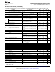
PACKAGE MATERIALS INFORMATION www.ti.com 24-Jul-2015 TAPE AND REEL INFORMATION *All dimensions are nominal Device Package Package Pins Type Drawing SPQ Reel Reel A0 Diameter Width (mm) (mm) W1 (mm) B0 (mm) K0 (mm) P1 (mm) W Pin1 (mm) Quadrant BQ24072RGTR QFN RGT 16 3000 330.0 12.4 3.3 3.3 1.1 8.0 12.0 Q2 BQ24072RGTR QFN RGT 16 3000 330.0 12.4 3.3 3.3 1.1 8.0 12.0 Q2 BQ24072RGTT QFN RGT 16 250 180.0 12.4 3.3 3.3 1.1 8.0 12.
PACKAGE MATERIALS INFORMATION www.ti.com 24-Jul-2015 *All dimensions are nominal Device Package Type Package Drawing Pins SPQ Length (mm) Width (mm) Height (mm) BQ24072RGTR QFN RGT 16 3000 367.0 367.0 35.0 BQ24072RGTR QFN RGT 16 3000 367.0 367.0 35.0 BQ24072RGTT QFN RGT 16 250 210.0 185.0 35.0 BQ24073RGTR QFN RGT 16 3000 367.0 367.0 35.0 BQ24073RGTT QFN RGT 16 250 210.0 185.0 35.0 BQ24074RGTR QFN RGT 16 3000 367.0 367.0 35.
IMPORTANT NOTICE Texas Instruments Incorporated and its subsidiaries (TI) reserve the right to make corrections, enhancements, improvements and other changes to its semiconductor products and services per JESD46, latest issue, and to discontinue any product or service per JESD48, latest issue. Buyers should obtain the latest relevant information before placing orders and should verify that such information is current and complete.