
Data Sheet

NCP1402
http://onsemi.com
3
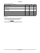
ABSOLUTE MAXIMUM RATINGS
Rating Symbol Value Unit
Power Supply Voltage (Pin 2) V
OUT
6.0 V
Input/Output Pins
LX (Pin 5)
LX Peak Sink Current
V
LX
I
LX
-0.3 to 6.0
400
V
mA
CE (Pin 1)
Input Voltage Range
Input Current Range
V
CE
I
CE
-0.3 to 6.0
-150 to 150
V
mA
Thermal Resistance, Junction-to-Air
R
JA
250 °C/W
Operating Ambient Temperature Range (Note 2) T
A
-40 to +85 °C
Operating Junction Temperature Range T
J
-40 to +125 °C
Storage Temperature Range T
stg
-55 to +150 °C
Stresses exceeding Maximum Ratings may damage the device. Maximum Ratings are stress ratings only. Functional operation above the
Recommended Operating Conditions is not implied. Extended exposure to stresses above the Recommended Operating Conditions may affect
device reliability.
NOTES:
1. This device series contains ESD protection and exceeds the following tests:
Human Body Model (HBM) ±2.0 kV per JEDEC standard: JESD22-A114.
Machine Model (MM) ±200 V per JEDEC standard: JESD22-A115.
2. The maximum package power dissipation limit must not be exceeded.
P
D
+
T
J(max)
* T
A
R
JA
3. Latchup Current Maximum Rating: ±150 mA per JEDEC standard: JESD78.
4. Moisture Sensitivity Level: MSL 1 per IPC/JEDEC standard: J-STD-020A.