
Data Sheet

NCP1402
http://onsemi.com
2
1
3
GND
CE
2
OUT
NC
4
LX
5
NCP1402
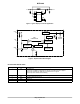
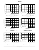
Figure 1. Typical Step-Up Converter Application
V
OUT
V
in
POWER
SWITCH
OUT
2
-
+
VOLTAGE
REFERENCE
SOFT-ST ART
PFM
CONTROLLER
PFM
OSCILLATOR
DRIVER
V
LX
LIMITER
PFM
COMPARATOR
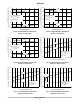
NC
3
GND
4
LX
5
1 CE
Figure 2. Representative Block Diagram
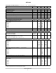
PIN FUNCTION DESCRIPTIONS
Pin # Symbol Pin Description
1 CE Chip Enable pin
(1) The chip is enabled if a voltage which is equal to or greater than 0.9 V is applied
(2) The chip is disabled if a voltage which is less than 0.3 V is applied
(3) The chip will be enabled if it is left floating
2 OUT Output voltage monitor pin, also the power supply pin of the device
3 NC No internal connection to this pin
4 GND Ground pin
5 LX External inductor connection pin to power switch drain