
Data Sheet

NCP1402
http://onsemi.com
15
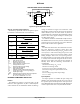
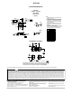
APPLICATIONS CIRCUIT INFORMATION
1
3
GND
CE
2
OUT
NC
4
LX
5
NCP1402
Figure 59. Typical Application Circuit
V
OUT
C2
68 F
D1
L1
47 H
C1
10 F
V
in
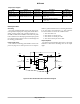
Step-up Converter Design Equations
NCP1402 step-up DC-DC converter designed to operate
in continuous conduction mode can be defined by:
Calculation Equation
L
v M
ǒ
V
in
2
V
OUT
I
Omax
Ǔ
I
PK
(V
in
* V
s)
t
on
L
) I
min
I
min
(t
on
) t
off
)I
O
t
off
*
(V
in
* V
S
)t
on
2L
t
off
(V
in
* V
s)
t
on
(V
OUT
) V
F
* V
in
)
Q
(I
L
* I
O
)t
off
V
ripple
[
Q
C
OUT
) (I
L
* I
O
)ESR
*NOTES:
I
PK
- Peak inductor current
I
min
- Minimum inductor current
I
O
- Desired dc output current
I
Omax
- Desired maximum dc output current
I
L
- Average inductor current
V
in
- Nominal operating dc input voltage
V
OUT
- Desired dc output voltage
V
F
- Diode forward voltage
V
S
- Saturation voltage of the internal FET switch
Q - Charge stores in the C
OUT
during charging up
V
ripple
- Output ripple voltage
ESR - Equivalent series resistance of the output capacitor
M - An empirical factor, when V
OUT
≥ 3.0 V,
M = 8 x 10
-6
, otherwise M = 5.3 x 10
-6
.
EXTERNAL COMPONENT SELECTION
Inductor
The NCP1402 is designed to work well with a 47 H
inductor in most applications. 47 H is a sufficiently low
value to allow the use of a small surface mount coil, but large
enough to maintain low ripple. Low inductance values
supply higher output current, but also increase the ripple and
reduce efficiency. Note that values below 27 H is not
recommended due to NCP1402 switch limitations. Higher
inductor values reduce ripple and improve efficiency, but
also limit output current.
The inductor should have small DCR, usually less than 1
to minimize loss. It is necessary to choose an inductor with
saturation current greater than the peak current which the
inductor will encounter in the application.
Diode
The diode is the main source of loss in DC-DC converters.
The most importance parameters which affect their
efficiency are the forward voltage drop, V
F
, and the reverse
recovery time, t
rr
. The forward voltage drop creates a loss
just by having a voltage across the device while a current
flowing through it. The reverse recovery time generates a
loss when the diode is reverse biased, and the current appears
to actually flow backwards through the diode due to the
minority carriers being swept from the P-N junction. A
Schottky diode with the following characteristics is
recommended:
Small forward voltage, V
F
< 0.3 V
Small reverse leakage current
Fast reverse recovery time/ switching speed
Rated current larger than peak inductor current,
I
rated
> I
PK
Reverse voltage larger than output voltage,
V
reverse
> V
OUT
Input Capacitor
The input capacitor can stabilize the input voltage and
minimize peak current ripple from the source. The value of
the capacitor depends on the impedance of the input source
used. Small Equivalent Series Resistance (ESR) Tantalum or
ceramic capacitor with value of 10 F should be suitable.