
Data Sheet

NEO-M8P - Data Sheet
UBX-15016656 - R06 Early Production Information Electrical specification
Page 21 of 30
For more information on how to noticeably reduce current consumption, see the Power Management
Application Note [5].
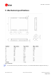
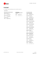
4.4 SPI timing diagrams
In order to avoid incorrect operation of the SPI, the user needs to comply with certain timing conditions. The
following signals need to be considered for timing constraints:
Symbol Description
SPI CS_N (SS_N) Slave select signal
SPI CLK (SCK) Slave clock signal
Table 12: Symbol description
Figure 6: SPI timing diagram
4.4.1 Timing recommendations
The recommendations below are based on a firmware running from Flash memory.
Parameter Description Recommendation
t
INIT
Initialization Time
>10 µs
t
DES
Deselect Time 1 ms
t
bit
Minimum bit time 180 ns (5.5 MHz max bit frequency)
t
byte
Minimum byte period
8 µs (125 kHz max byte frequency)
Table 13: SPI timing recommendations
The values in the above table result from the requirement of an error-free transmission. For more
information see the u-blox 8 / u-blox M8 Receiver Description Including Protocol Specification [2].
4.5 DDC timing
The DDC interface is I
2
C Fast Mode compliant. For timing parameters consult the I
2
C standard.
The maximum bit rate is 400 kb/s. The interface stretches the clock when slowed down when serving
interrupts, so real bit rates may be slightly lower.