
Data Sheet

Page 5
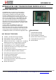
RFM69HCW
Tel: + 86-755-82973805 Fax: +86- 755-82973550 E-mail: sales@hoperf.com http:/ / www.hoperf.com
Index of Figures Page
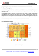
Figure 1. Block Diagram
................................................................................................................................................
8
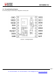
Figure 2. Pin Diagram
....................................................................................................................................................
9
Figure 3. Marking Diagram
............................................................................................................................................
9
Figure 4. TCXO Connection
........................................................................................................................................
16
Figure 5. Transmitter Block Diagram
...........................................................................................................................
19
Figure 6. Output Power Curves
...................................................................................................................................
22
Figure 7. Receiver Block Diagram
...............................................................................................................................
23
Figure 8. AGC Thresholds Settings
.............................................................................................................................
24
Figure 9. RSSI Dynamic Curve
....................................................................................................................................
28
Figure 10. Cordic Extraction
........................................................................................................................................
28
Figure 11. OOK Peak Demodulator Description
..........................................................................................................
29
Figure 12. Floor Threshold Optimization
.....................................................................................................................
30
Figure 13. Bit Synchronizer Description
......................................................................................................................
31
Figure 14. FEI Process
................................................................................................................................................
32
Figure 15. Optimized AFC (AfcLowBetaOn=1)
............................................................................................................
33
Figure 16. Temperature Sensor Response
.................................................................................................................
34
Figure 17. Tx Startup, FSK and OOK
..........................................................................................................................
36
Figure 18. Rx Startup - No AGC, no AFC
....................................................................................................................
37
Figure 19. Rx Startup - AGC, no AFC
.........................................................................................................................
37
Figure 20. Rx Startup - AGC and AFC
........................................................................................................................
37
Figure 21. Listen Mode Sequence (no wanted signal is received)
..............................................................................
39
Figure 22. Listen Mode Sequence (wanted signal is received)
...................................................................................
41
Figure 23. Auto Modes of Packet Handler
...................................................................................................................
42
Figure 24. RFM69HCW Data Processing Conceptual View
...........................................................................................
43
Figure 25. SPI Timing Diagram (single access)
..........................................................................................................
44
Figure 26. FIFO and Shift Register (SR)
.....................................................................................................................
45
Figure 27. FifoLevel IRQ Source Behavior
..................................................................................................................
46
Figure 28. Sync Word Recognition
..............................................................................................................................
47
Figure 29. Continuous Mode Conceptual View
...........................................................................................................
49
Figure 30. Tx Processing in Continuous Mode
............................................................................................................
49
Figure 31. Rx Processing in Continuous Mode
...........................................................................................................
50
Figure 32. Packet Mode Conceptual View
...................................................................................................................
51
Figure 33. Fixed Length Packet Format
......................................................................................................................
52
Figure 34. Variable Length Packet Format
..................................................................................................................
52
Figure 35. Unlimited Length Packet Format
................................................................................................................
53
Figure 36. CRC Implementation
..................................................................................................................................
58
Figure 37. Manchester Encoding/Decoding
.................................................................................................................
58
Figure 38. Data Whitening
...........................................................................................................................................
59
Figure 39. POR Timing Diagram
.................................................................................................................................
75
Figure 40. Manual Reset Timing Diagram
...................................................................................................................
76