
Data Sheet


DocID009413 Rev 9 19/30
TSH80, TSH81, TSH82, TSH84 Test conditions
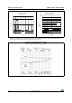
4 Test conditions
4.1 Layout precautions
To make the best use of the TSH8x circuits at high frequencies, some precautions have to
be taken with regard to the power supplies.
• In high-speed circuit applications, the implementation of a proper ground plane on both
sides of the PCB is mandatory to ensure low inductance and low resistance common
return.
• Power supply bypass capacitors (4.7 µF and ceramic 100 pF) should be placed as
close as possible to the IC pins in order to improve high frequency bypassing and
reduce harmonic distortion. The power supply capacitors must be incorporated for both
the negative and positive pins.
• All inputs and outputs must be properly terminated with output resistors. Thus, the
amplifier load is resistive only and the stability of the amplifier is improved.
All leads must be wide and must be as short as possible, especially for op-amp inputs
and outputs, in order to decrease parasitic capacitance and inductance.
• Time constants result from parasitic capacitance. To reduce time constants in lower-
gain applications, use a low feedback resistance (under 1 kΩ).
• Choose the smallest component size possible (SMD).
• On the output, the load capacitance must be negligible to maintain good stability. Place
ca serial resistance as close as possible to the output pin to minimize the effect of the
load capacitance.
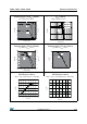
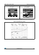
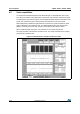
Figure 32. CCIR330 video line