
Data Sheet

PCA9615 All information provided in this document is subject to legal disclaimers. © NXP Semiconductors N.V. 2016. All rights reserved.
Product data sheet Rev. 1.1 — 10 May 2016 9 of 29
NXP Semiconductors
PCA9615
2-channel multipoint Fm+ dI
2
C-bus buffer with hot-swap logic
8. Application design-in information
8.1 I
2
C-bus
As with the standard I
2
C-bus system, pull-up resistors are required to provide the logic
HIGH levels on the single-ended buffered bus (standard open-drain configuration of the
I
2
C-bus). The size of these pull-up resistors depends on the system. The device is
designed to work with Standard-mode, Fast-mode and Fast-mode Plus I
2
C-bus devices in
addition to SMBus devices. Standard-mode and Fast-mode I
2
C-bus and SMBus devices
only specify 3 mA output drive; this limits the termination current to 3 mA in a generic
I
2
C-bus system where Standard-mode devices and multiple masters are possible. When
only Fast-mode Plus devices are used, then higher termination currents can be used due
to their 30 mA sink capability.
8.2 Differential I
2
C-bus application
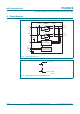
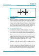
See Figure 7 through Figure 9.
The simple application (Figure 7
) shows an existing SMBus/I
2
C-bus being extended over
a section of dI
2
C-bus transmission line, containing a dedicated twisted pair for SCL and
SDA. At one end of the transmission line, a resistor network (R1-R2-R1) terminates the
twisted-pair cable and biases D+ positive with respect to D. An identical resistor network
at the other end of the transmission line terminates the twisted-pair cable. DC power for
each end of the transmission line and the V
DD(B)
of each PCA9615 bus buffer can be from
separate and isolated power supplies, or use the same supply and ground run in separate
wires along the same path as the dI
2
C-bus signal twisted pairs.
Telecom category 5 (‘CAT 5’) data cable is well suited for this task, but loose wires may
also be used, with a reduction in performance. Assuming V
DD(B)
is 5 V, and using CAT 5
cable, R2 is 120 , R1 is 600 . The parallel combination yields a termination of 100 at
each end of the twisted pairs.
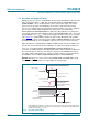
Either side of the dI
2
C-bus buffer pair is connected to standard SMBus/I
2
C buses, which
require their own pull-up resistors to V
DD(A)
of the PCA9615 bus buffers. V
DD(A)
and V
DD(B)
can be the same supply, however, making them different voltages enables the PCA9615
bus buffers to level translate between the SMBus/I
2
C-bus and dI
2
C-bus sections of the
bus, or to have different supply voltages and level translate at either end of the dI
2
C-bus
and SMBus/I
2
C-bus system.
For example, the left-hand bus master (and local slave) may operate on a 3.3 V supply
and SMBus/I
2
C-bus while the dI
2
C-bus transmission lines are at 5 V, and the right-hand
slave is operated from a different 3.3 V supply and SMBus/I
2
C-bus, or even a different bus
voltage other than 3.3 V.
Depending upon the timing from the system master, clock toggle rates can vary from
10 kHz for the SMBus (or less for SMBus/I
2
C-bus protocol) up to 100 kHz (Standard
mode), 400 kHz (Fast mode), or up to 1 MHz (Fast-mode Plus).
The bus path is bidirectional. Assume that the left side SMBus/I
2
C-bus becomes active. A
START condition (SDA goes LOW while SDA is HIGH) is sent. This upsets the idle
condition on the dI
2
C-bus section of the bus, because D+ was more positive than D and