
Data Sheet

xxxxxxxxxxxxxxxxxxxxx xxxxxxxxxxxxxxxxxxxxxxxxxx xxxxxxx x x x xxxxxxxxxxxxxxxxxxxxxxxxxxxxxx xxxxxxxxxxxxxxxxxxx xx xx xxxxx
xxxxxxxxxxxxxxxxxxxxxxxxxxx xxxxxxxxxxxxxxxxxxx xxxxxx xxxxxxxxxxxxxxxxxxxxxxxxxxxxxxxxxxx xxxxxxxxxxxx x x
xxxxxxxxxxxxxxxxxxxxx xxxxxxxxxxxxxxxxxxxxxxxxxxxxxx xxxxx xxxxxxxxxxxxxxxxxxxxxxxxxxxxxxxxxxxxxxxxxxxxxxxxxx xxxxxxxx
xxxxxxxxxxxxxxxxxxxxxxxxx xxxxxxxxxxxxxxxxxxxx xxx
PCA9615 All information provided in this document is subject to legal disclaimers. © NXP Semiconductors N.V. 2016. All rights reserved.
Product data sheet Rev. 1.1 — 10 May 2016 12 of 29
NXP Semiconductors
PCA9615
2-channel multipoint Fm+ dI
2
C-bus buffer with hot-swap logic
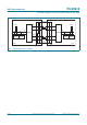
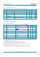
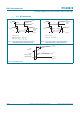
Remark: Keep drops as short as possible.
Remark: There is only one ground pin on the PCA9615, so the single-ended I
2
C-bus signals that are not ground offset tolerant must be referenced to the ground pin on
the part. And any ground offset must be on the differential side where the differential input and output can tolerate a ground offset of up to 0.5 V
DD(B)
.
Fig 8. PCA9615 application diagram; V
DD
and V
SS
are routed through the cable
V
DD(B)
PCA9615
SCL
SDA
SLAVE
MASTER
DSCLP
DSCLM
DSDAP
DSDAM
V
SS
002aah768
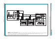
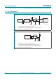
CARD
PCA9615
SLAVE MASTER
CARD
PCA9615
V
SS
V
DD
V
SS
V
DD
PCA9615
SLAVE
MASTER
CARD
optional
V
DD(B)
V
DD(B)
termination
V
DD(A)
V
DD(A)
SLAVE MASTER
CARD
V
DD(A)
V
DD(A)