
Data Sheet

PCA9615 All information provided in this document is subject to legal disclaimers. © NXP Semiconductors N.V. 2016. All rights reserved.
Product data sheet Rev. 1.1 — 10 May 2016 10 of 29
NXP Semiconductors
PCA9615
2-channel multipoint Fm+ dI
2
C-bus buffer with hot-swap logic
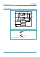
now they are reversed. The right side bus buffer sees the differential lines change polarity
and in turn pulls SDA LOW on the SMBus/I
2
C-bus side of the bus buffer, transmitting the
START condition to the slave on that section of the SMBus/I
2
C-bus.
If the data clocked out by the left side master contains a valid address of the right side
slave, that slave responds by pulling SDA LOW on the ninth clock. This condition is
transmitted across the dI
2
C-bus section that has now changed flow direction, and
received by the left side bus buffer (again, D+ was more positive than D and now they
are reversed).
This sequence continues until the master sends the STOP condition (SCL HIGH while
SDA goes HIGH), placing the active slave (on the right side) back to idle. When idle, the
normal SMBus/I
2
C-bus (both left and right sections) are pulled up by their respective
pull-ups. In turn, the dI
2
C-bus section of the bus rests with D+ more positive than D.
The idle condition can be changed by any node on either SMBus/I
2
C-bus section or an
additional dI
2
C-bus node, if present, on the dI
2
C-bus section of the system. This allows
the existing SMBus/I
2
C-bus protocol to operate transparently over a mix of SMBus/I
2
C
and dI
2
C bus segments.
Due to the SMBus/I
2
C-bus handshake protocol (ACK/NACK on the ninth clock pulse), the
direction of the SMBus/I
2
C-bus is reversed often. The ‘time of flight’ for the signals to pass
through each bus buffer and for the target slave to respond defines the maximum speed of
the bus, regardless of how fast the clock toggles. The dI
2
C-bus section of the bus requires
two additional PCA9615 bus buffers, further delaying the SMBus/I
2
C-bus traffic. If the
dI
2
C-bus transmission line section is made longer, the bus operates much slower,
regardless of the clock toggle speed.
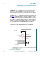
It is not necessary to have a ground connection between each end of the dI
2
C section of
the bus. The dI
2
C-bus receiver responds to reversal of the polarity of the D+ and D
signals, and ignores the common-mode voltage that may be present.
Ideally, the common-mode voltage is the same at each end of the twisted pairs, and no
current flows along the twisted pair when the bus is idle, because the D+ and D dI
2
C-bus
drivers are both high-impedance, the bus is biased by R1-R2-R1 at each end. If the
common-mode voltage is not 0 V, current flows along the twisted pair, returning through
the common ground or common power supply connection if present.
If both ends of the twisted pair are powered by the same V
DD(B)
supply and one end is
remote, there will be a common-mode offset between them. This is ignored by the
dI
2
C-bus receivers, which only respond to the difference between D+ and D.
However, a large common-mode offset voltage forces the D+ and D signals out of the
range of the receiver, and data are lost. The PCA9615 bus buffers use standard ESD
protection networks to protect the external pins, and therefore should not be biased above
or below the V
DD(B)
and V
SS
pins respectively. This limits the common-mode range to
approximately 0.5 V
DD(B)
.
DC resistance of the transmission line attenuates the signals, more so over longer
distances. The loss of signal amplitude is made up by the gain of the dI
2
C-bus receiver.
There is a limit to how long the dI
2
C-bus section can be made, as it is necessary for the
driver to overcome the bias on the transmission line, in order to signal a polarity change
(D+ and D reversal) at the receiver end.