
Data Sheet


MCP4725
DS22039D-page 4 © 2009 Microchip Technology Inc.
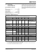
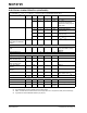
Power Up Time T
PU
—2.5 — µsV
DD
= 5V
—5 — µsV
DD
= 3V
Exit Power-down Mode,
(Started from falling edge of
ACK pulse)
DC Output Impedance R
OUT
—1 — Ω Normal mode (V
OUT
to V
SS
)
—1 — kΩ Power-Down Mode 1
(V
OUT
to V
SS
)
—100 — kΩ Power-Down Mode 2
(V
OUT
to V
SS
)
—500 — kΩ Power-Down Mode 3
(V
OUT
to V
SS
)
Supply Voltage Power-up
Ramp Rate for EEPROM
loading
V
DD_RAMP
1 — — V/ms Validation only.
Dynamic Performance
Major Code Transition
Glitch
— 45 — nV-s 1 LSB change around major
carry (from 800h to 7FFh)
(Note 2)
Digital Feedthrough — <10 — nV-s Note 2
Digital Interface
Output Low Voltage V
OL
— — 0.4 V I
OL
= 3 mA
Input High Voltage
(SDA and SCL Pins)
V
IH
0.7V
DD
—— V
Input Low Voltage
(SDA and SCL Pins)
V
IL
—
—0.3V
DD
V
Input High Voltage
(A0 Pin)
V
A0-Hi
0.8V
DD
—— Note 4
Input Low Voltage
(A0 Pin)
V
A0-IL
— — 0.2V
DD
Note 4
Input Leakage I
LI
— — ±1 µA SCL = SDA = A0 = V
SS
or
SCL = SDA = A0 = V
DD
Pin Capacitance C
PIN
—— 3 pF Note 2
EEPROM
EEPROM Write Time T
WRITE —25 50 ms
Data Retention — 200 — Years At +25°C, (Note 2)
Endurance 1 — — Million
Cycles
At +25°C, (Note 2)
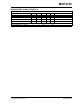
ELECTRICAL CHARACTERISTICS (CONTINUED)
Electrical Specifications: Unless otherwise indicated, all parameters apply at V
DD
= + 2.7V to 5.5V, V
SS
= 0V,
R
L
= 5 kΩ from V
OUT
to V
SS
, C
L
= 100 pF, T
A
= -40°C to +125°C. Typical values are at +25°C.
Parameter Sym Min Typ Max Units Conditions
Note 1: Test Code Range: 100 to 4000.
2: This parameter is ensure by design and not 100% tested.
3: Within 1/2 LSB of the final value when code changes from 1/4 to 3/4 (400h to C00h) of full scale range.
4: Logic state of external address selection pin (A0 pin).