
Data Sheet


© 2009 Microchip Technology Inc. DS22039D-page 35
MCP4725
8.5.2 DECREASING THE OUTPUT STEP
SIZE
Calibrating the threshold of a diode, transistor or
resistor may require a very small step size in the DAC
output voltage. These applications may require about
200 µV of step resolution within 0.8V of range.
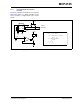
One method of achieving this small step resolution is
using a voltage divider at the DAC output. An example
is shown in Example 8-1. The step size of the DAC
output is scaled down by the factor of the ratio of the
voltage divider. Note that the bypass capacitor on the
output of the voltage divider plays a critical function in
attenuating the output noise of the DAC and the
induced noise from the environment.
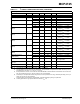
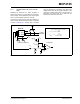
EXAMPLE 8-1: Set Point Or Threshold Calibration.
To MCU
(MASTER)
R
R
V
DD
Comparator
R
1
R
2
0.1 µF
V
TRIP
R
SENSE
MCP4725
V
DD
V
OUT
A0
SCL
V
SS
1
2
3
4
5
6
V
DD
SDA
10 µF0.1 µF
V
DD
Dn Input Code (0 to 4095)=
V
OUT
V
DD
Dn
4096
------------
×
=
V
TRIP
V
OUT
R
2
R
1
R
2
+
-------------------
⎝⎠
⎛⎞
=
Light
(Ceramic) (Tantalum)