
Data Sheet


© 2009 Microchip Technology Inc. DS22039D-page 33
MCP4725
8.0 TYPICAL APPLICATIONS
The MCP4725 device is one of Microchip’s latest DAC
device family with non-volatile EEPROM memory. The
device is a general purpose resistive string DAC
intended to be used in applications where a precision,
and low power DAC with moderate bandwidth is
required.
Since the device includes non-volatile EEPROM
memory, the user can use this device for applications
that require the output to return to the previous set-up
value on subsequent power-ups.
Applications generally suited for the MCP4725 device
family include:
• Set Point or Offset Trimming
• Sensor Calibration
• Portable Instrumentation (Battery Powered)
• Motor Speed Control
8.1 Connecting to I
2
C BUS using
Pull-Up Resistors
The SCL and SDA pins of the MCP4725 are open-drain
configurations. These pins require a pull-up resistor as
shown in Figure 8-1. The value of these pull-up
resistors depends on the operating speed (standard,
fast, and high speed) and loading capacitance of the
I
2
C bus line. Higher value of pull-up resistor consumes
less power, but increases the signal transition time
(higher RC time constant) on the bus. Therefore, it can
limit the bus operating speed. The lower resistor value,
on the other hand, consumes higher power, but allows
higher operating speed. If the bus line has higher
capacitance due to long bus line or high number of
devices connected to the bus, a smaller pull-up resistor
is needed to compensate the long RC time constant.
The pull-up resistor is typically chosen between 1 kΩ
and 10 kΩ ranges for standard and fast modes, and
less than 1 kΩ for high speed mode.
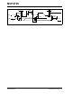
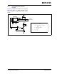
FIGURE 8-1: I
2
C Bus Interface
Connection with A0 pin tied to V
SS
.
Two devices with the same A2 and A1 address bits can
be connected to the same I
2
C bus by utilizing the A0
address pin (Example: A0 pin of device A is tied to V
DD
,
and the other device’s pin is tied to V
SS
).
8.1.1 DEVICE CONNECTION TEST
The user can test the presence of the MCP4725 on the
I
2
C bus line without performing the data conversion.
This test can be achieved by checking an acknowledge
response from the MCP4725 after sending a read or
write command. Here is an example using Figure 8-2:
(a) Set the R/W
bit “HIGH” in the address byte.
(b) If the MCP4725 is connected to the I
2
C bus line, it
will then acknowledge by pulling SDA bus LOW
during the ACK clock and then release the bus
back to the I
2
C Master.
(c) A STOP or repeated START bit can then be issued
from the Master and I
2
C communication can
continue.
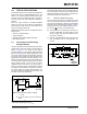
FIGURE 8-2: I
2
C Bus Connection Test.
MCP4725
V
OUT
A0
SCL
V
SS
1
2
3
4
5
6
V
DD
SDA
10 µF0.1 µF
R
R
Analog
V
DD
V
DD
To MCU
(MASTER)
Output
Note 1: R is the pull-up resistor. Typically
1 ~ 10 kΩ
2: A0 can be tied to V
SS
, V
DD
or driven by
MCU
12345678 9
SCL
SDA
11
0
0A2A1A0
1
START
Bit
Address Byte
Address bits
Device bits
R/W
START
Bit
MCP4725
ACK
Response