
Data Sheet


MCP4725
DS22039D-page 26 © 2009 Microchip Technology Inc.
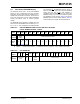
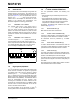
6.2 READ COMMAND
If the R/W bit is set to a logic “high”, then the device
outputs on SDA pin, the DAC register and EEPROM
data. Figure 6-3 shows an example of reading the
register and EEPROM data. The 2nd byte in Figure 6-
3 indicates the current condition of the device
operation. The RDY/BSY
bit indicates EEPROM
writing status. The RDY/BSY bit stays low during
EEPROM writng and high when the writing is
completed.
FIGURE 6-3: Read Command and Output Data Format.
1st byte
ACK (MCP4725)
2nd byte 3rd byte
ACK (Master)
4th byte
D3 D2 D0D11 1 0 0 A2 A1 A0 1
RDY/
XXXPD1PD0X XXXXD11 D10 D9 D8 D7 D6 D5 D4
START Bit
Device Code Address Bits
R/W
5th byte 6th byte
D7 D6 D4D5 D3 D2 D1 D0X PD1 PD0 X D11 D10 D9 D8
STOP
Bit
Note 1: Bytes 2 - 6 are repeated in repeat bytes after byte 6.
2: X is don’t care bit.
Read Command
DAC register Data (12 bits)
in DAC Register
Current Settings
See Note 2
EEPROM Write Status Indicate Bit
(1: Completed, 0: Incomplete)
BSY
EEPROM Data
POR
ACK (Master)
ACK (Master)