
Data Sheet


MCP4725
DS22039D-page 20 © 2009 Microchip Technology Inc.
5.4.2 V
DD
RAMP RATE AND EEPROM
The MCP4725 uploads the EEPROM data to the DAC
register during power-up sequence. However, if the
V
DD
ramp rate is too slow ( <1 V/ms), the device may
not be able to load the EEPROM data to the DAC
register. Therefore, the DAC output that is correspond-
ing to the current EEPROM data may not available to
the output pin. It is highly recommended to send a Gen-
eral Call Reset Command (see Section 7.3.1 “Gen-
eral call reset”) after power-up. This command will
reset the device at a stable V
DD
and make the DAC out-
put available immediately using the EEPROM data.
5.5 Normal and Power-Down Modes
The device has two modes of operation: Normal mode
and power-down mode. The mode is selected by
programming the power-down bits (PD1 and PD0) in
the Configuration register. The user can also program
the two power-down bits in non-volatile EEPROM
memory.
When the normal mode is selected, the device
operates a normal digital-to-analog conversion. If the
power-down mode is selected, the device enters a
power saving condition by shutting down most of the
internal circuits. During the power-down mode, all
internal circuits except the I
2
C interface are disabled
and there is no data conversion event, and no V
OUT
is
available. The device also switches the output stage
from the output of the amplifier to a known resistive
load. The value of the resistive load is determined by
the state of the power-down bits (PD1 and PD0).
Table 5-2 shows the outcome of the power-down bit
and the resistive load.
During the power-down mode, the device draws about
60 nA (typical). Although most of internal circuits are
shutdown, the serial interface remains active in order
to receive the I
2
C command.
The device exits the power-down mode immediately
when (a) it receives a new write command for normal
mode or (b) it receives an I
2
C General Call Wake-Up
Command.
When the DAC operation mode is changed from
power-down to normal mode, the output settling time
takes less than 10 µs, but greater than the standard
Active mode settling time (6 µs, typical).
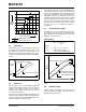
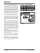
TABLE 5-2: POWER-DOWN BITS
FIGURE 5-1: Output Stage for Power-
Down Mode.
PD1 PD0 Function
00Normal Mode
011kΩ resistor to ground
(1)
10100 kΩ resistor to ground
(1)
11500 kΩ resistor to ground
(1)
Note 1: In the power-down mode: V
OUT
is off and
most of internal circuits are disabled.
1kΩ
100 kΩ 500 kΩ
Power-Down
Control Circuit
Resistive
Load
V
OUT
OP
Amp
Resistive String DAC