
Data Sheet


© 2009 Microchip Technology Inc. DS22039D-page 13
MCP4725
3.0 PIN DESCRIPTIONS
The descriptions of the pins are listed in Table 3-1.
3.1 Analog Output Voltage (V
OUT
)
V
OUT
is an analog output voltage from the DAC device.
DAC output amplifier drives this pin with a range of V
SS
to V
DD
.
3.2 Supply Voltage (V
DD
or V
SS
)
V
DD
is the power supply pin for the device. The voltage
at the V
DD
pin is used as the supply input as well as the
DAC reference input. The power supply at the V
DD
pin
should be clean as possible for a good DAC
performance.
This pin requires an appropriate bypass capacitor of
about 0.1 µF (ceramic) to ground. An additional 10 µF
capacitor (tantalum) in parallel is also recommended to
further attenuate high frequency noise present in
application boards. The supply voltage (V
DD
) must be
maintained in the 2.7V to 5.5V range for specified
operation.
V
SS
is the ground pin and the current return path of the
device. The user must connect the V
SS
pin to a ground
plane through a low impedance connection. If an
analog ground path is available in the application PCB
(printed circuit board), it is highly recommended that
the V
SS
pin be tied to the analog ground path or
isolated within an analog ground plane of the circuit
board.
3.3 Serial Data Pin (SDA)
SDA is the serial data pin of the I
2
C interface. The SDA
pin is used to write or read the DAC register and
EEPROM data. The SDA pin is an open-drain N-chan
nel driver. Therefore, it needs a pull-up resistor from the
V
DD
line to the SDA pin. Except for START and STOP
conditions, the data on the SDA pin must be stable
during the high period of the clock. The high or low
state of the SDA pin can only change when the clock
signal on the SCL pin is low. Refer to Section 7.0 “I
2
C
Serial Interface Communication” for more details of
I
2
C Serial Interface communication.
3.4 Serial Clock Pin (SCL)
SCL is the serial clock pin of the I
2
C interface. The
MCP4725 acts only as a slave and the SCL pin accepts
only external serial clocks. The input data from the
Master device is shifted into the SDA pin on the rising
edges of the SCL clock and output from the MCP4725
occurs at the falling edges of the SCL clock. The SCL
pin is an open-drain N-channel driver. Therefore, it
needs a pull-up resistor from the V
DD
line to the SCL
pin. Refer to Section 7.0 “I
2
C Serial Interface Com-
munication” for more details of I
2
C Serial Interface
communication.
3.5 Device Address Selection Pin (A0)
This pin is used to select the A0 address bit by the user.
The user can tie this pin to V
SS
(logic ‘0’), or V
DD
(logic ‘1’), or can be actively driven by the digital logic
levels, such as the I
2
C Master Output. See Section 7.2
“Device Addressing” for more details of the address
bits.
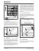
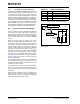
TABLE 3-1: PIN FUNCTION TABLE
MCP4725
Name Description
SOT-23
1V
OUT
Analog Output Voltage
2V
SS
Ground Reference
3V
DD
Supply Voltage
4SDAI
2
C Serial Data
5SCLI
2
C Serial Clock Input
6A0I
2
C Address Bit Selection pin (A0 bit). This pin can be tied to V
SS
or V
DD
, or can be
actively driven by the digital logic levels. The logic state of this pin determines what
the A0 bit of the I
2
C address bits should be.