MCP4725 12-Bit Digital-to-Analog Converter with EEPROM Memory in SOT-23-6 Features DESCRIPTION • • • • • • • • • • • The MCP4725 is a low-power, high accuracy, single channel, 12-bit buffered voltage output Digital-toAnalog Convertor (DAC) with non-volatile memory (EEPROM). Its on-board precision output amplifier allows it to achieve rail-to-rail analog output swing. 12-Bit Resolution On-Board Non-Volatile Memory (EEPROM) ±0.
MCP4725 NOTES: DS22039D-page 2 © 2009 Microchip Technology Inc.
MCP4725 1.0 ELECTRICAL CHARACTERISTICS † Notice: Stresses above those listed under “Maximum ratings” may cause permanent damage to the device. This is a stress rating only and functional operation of the device at these or any other conditions above those indicated in the operation listings of this specification is not implied. Exposure to maximum rating conditions for extended periods may affect device reliability Absolute Maximum Ratings† VDD.............................................................
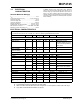
MCP4725 ELECTRICAL CHARACTERISTICS (CONTINUED) Electrical Specifications: Unless otherwise indicated, all parameters apply at VDD = + 2.7V to 5.5V, VSS = 0V, RL = 5 kΩ from VOUT to VSS, CL = 100 pF, TA = -40°C to +125°C. Typical values are at +25°C. Parameter Power Up Time Sym Typ Max Units Conditions — 2.
MCP4725 TEMPERATURE CHARACTERISTICS Electrical Specifications: Unless otherwise indicated, VDD = +2.7V to +5.5V, VSS = GND. Parameters Sym Min Typ Max Units Specified Temperature Range TA -40 — +125 °C Operating Temperature Range TA -40 — +125 °C Storage Temperature Range TA -65 — +150 °C θJA — 190.5 — °C/W Conditions Temperature Ranges Thermal Package Resistances Thermal Resistance, 6L-SOT-23 © 2009 Microchip Technology Inc.
MCP4725 NOTES: DS22039D-page 6 © 2009 Microchip Technology Inc.
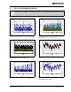
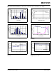
MCP4725 2.0 TYPICAL PERFORMANCE CURVES Note: The graphs and tables provided following this note are a statistical summary based on a limited number of samples and are provided for informational purposes only. The performance characteristics listed herein are not tested or guaranteed. In some graphs or tables, the data presented may be outside the specified operating range (e.g., outside specified power supply range) and therefore, outside the warranted range. 0.16 0.4 0.12 0.3 VDD = 2.
MCP4725 Note: Unless otherwise indicated, TA = +25°C, VDD = +5.0V, VSS = 0V, RL = 5 kΩ to VSS, CL = 100 pF. 2 +25°C 2 Output Error (mV) 1 3 - 40°C INL(LSB) 0 -1 -2 -3 +85°C -4 TA = -40 C TA = 85 C +125°C -5 0 1024 3072 -1 -2 VDD = 5.5V -3 -5 -40 -25 -10 4096 5 20 35 50 65 80 95 110 125 Temperature (°C) FIGURE 2-7: INL vs. Code and Temperature (VDD = 2.7V). FIGURE 2-10: Output Error vs. Temperature (Code = 4000d). 3 450 400 350 VDD = 5.
MCP4725 100 90 80 70 60 50 40 30 20 10 0 6 VDD = 5V VOUT (V) 5 VDD = 5V Code = FFFh 4 3 2 0 236 232 228 224 220 216 212 208 204 200 196 192 188 184 1 180 Occurance Note: Unless otherwise indicated, TA = +25°C, VDD = +5.0V, VSS = 0V, RL = 5 kΩ to VSS, CL = 100 pF. 0 1 2 Current (µA) FIGURE 2-12: FIGURE 2-15: IDD Histogram . 6 80 VDD = 2.7V 70 5 VOUT vs. Resistive Load.
MCP4725 VIL Threshold (V) Note: Unless otherwise indicated, TA = +25°C, VDD = +5.0V, VSS = 0V, RL = 5 kΩ to VSS, CL = 100 pF. Half Scale Code Change: 000h to 7FFh 2.50 2.30 2.10 1.90 1.70 1.50 1.30 1.10 0.90 0.70 0.50 VOUT (2V/Div) VDD = 5.5V VDD = 5.0V VDD = 2.7V -40 -25 -10 5 CLK 20 35 50 65 80 95 110 125 Time (2 µs/Div) Temperature (°C) FIGURE 2-18: VIN Low Threshold vs. Temperature and VDD. Full Scale Code Change: 000h to FFFh FIGURE 2-21: Half Scale Settling Time.
MCP4725 Note: Unless otherwise indicated, TA = +25°C, VDD = +5.0V, VSS = 0V, RL = 5 kΩ to VSS, CL = 100 pF. VOUT (2V/Div) CLK Time (2 µs/Div) FIGURE 2-24: Exiting Power Down Mode. © 2009 Microchip Technology Inc.
MCP4725 NOTES:. DS22039D-page 12 © 2009 Microchip Technology Inc.
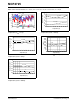
MCP4725 3.0 PIN DESCRIPTIONS The descriptions of the pins are listed in Table 3-1. TABLE 3-1: MCP4725 SOT-23 1 3.1 PIN FUNCTION TABLE Name VOUT Description Analog Output Voltage 2 VSS 3 VDD Ground Reference Supply Voltage 4 SDA I2C Serial Data 5 SCL I2C Serial Clock Input 6 A0 I2C Address Bit Selection pin (A0 bit). This pin can be tied to VSS or VDD, or can be actively driven by the digital logic levels.
MCP4725 NOTES: DS22039D-page 14 © 2009 Microchip Technology Inc.
MCP4725 4.0 TERMINOLOGY 4.1 Resolution The resolution is the number of DAC output states that divide the full scale range. For the 12-bit DAC, the resolution is 212 or the DAC code ranges from 0 to 4095. 4.2 LSB 7 INL = - 1 LSB 5 Analog 4 Output (LSB) 3 INL = 0.5 LSB 2 The least significant bit or the ideal voltage difference between two successive codes.
MCP4725 7 DNL = 0.5 LSB 6 5 DNL = 2LSB Analog 4 Output (LSB) 3 In the MCP4725, the gain error is not calibrated at the factory and most of the gain error is contributed by the output op amp saturation near the code range beyond 4000. For the applications which need the gain error specification less than 1% maximum, the user may consider using the DAC code range between 100 and 4000 instead of using full code range (code 0 to 4095).
MCP4725 4.9 Offset Error Drift Offset error drift is the variation in offset error due to a change in ambient temperature. The offset error drift is typically expressed in ppm/oC. 4.10 Settling Time The Settling time is the time delay required for the DAC output to settle to its new output value from the start of code transition, within specified accuracy. In the MCP4725, the settling time is a measure of the time delay until the DAC output reaches its final value (within 0.
MCP4725 NOTES: DS22039D-page 18 © 2009 Microchip Technology Inc.
MCP4725 5.0 GENERAL DESCRIPTION The MCP4725 is a single channel buffered voltage output 12-bit DAC with non-volatile memory (EEPROM). The user can store configuration register bits (2 bits) and DAC input data (12 bits) in non-volatile EEPROM (14 bits) memory. When the device is powered on first, it loads the DAC code from the EEPROM and outputs the analog output accordingly with the programmed settings. The user can reprogram the EEPROM or DAC register any time.
MCP4725 5.4.2 VDD RAMP RATE AND EEPROM The MCP4725 uploads the EEPROM data to the DAC register during power-up sequence. However, if the VDD ramp rate is too slow ( <1 V/ms), the device may not be able to load the EEPROM data to the DAC register. Therefore, the DAC output that is corresponding to the current EEPROM data may not available to the output pin. It is highly recommended to send a General Call Reset Command (see Section 7.3.1 “General call reset”) after power-up.
MCP4725 5.6 Non-Volatile EEPROM Memory are transferred to the EEPROM memory block. A status bit, RDY/BSY, stays low during the EEPROM writing and goes high as the write operation is completed. While the RDY/BSY bit is low (during the EEPROM writing), any new write command is ignored (for EEPROM or DAC register). Table 5-3 shows the EEPROM bits and factory default settings. Table 5-4 shows the DAC input register bits of the MCP4725.
MCP4725 NOTES: DS22039D-page 22 © 2009 Microchip Technology Inc.
MCP4725 6.0 THEORY OF OPERATION When the device is connected to the I2C bus line, the device is working as a slave device. The Master (MCU) can write/read the DAC input register or EEPROM using the I2C interface command. The MCP4725 device address contains four fixed bits ( 1100 = device code) and three address bits (A2, A1, A0). The A2 and A1 bits are hard-wired during manufacturing, and A0 bit is determined by the logic state of A0 pin.
MCP4725 TABLE 6-2: WRITE COMMAND TYPE C 2 C 1 C0 Command Name 0 0 X Fast Mode 0 0 0 0 1 1 X 0 1 Function This command is used to change the DAC register.
MCP4725 (A) Write DAC Register: (C2, C1, C0) = (0,1,0) or STOP Bit (B) Write DAC Register and EEPROM: (C2, C1, C0) = (0,1,1) ACK (MCP4725) 1st byte (Device Addressing) 1 1 0 0 A2 A1 A0 0 2nd byte C2 C1 C0 X X 3rd byte PD1 PD0 X 4th byte D11 D10 D9 D8 D7 D6 D5 D4 Unused Unused Device Code Address Bits R/W START Bit ACK (MCP4725) D3 D2 D1 D0 X X X X DAC Register Data (12 bits) Unused Power Down Selection Write Command Type: Write DAC Register: (C2 = 0, C1 = 1, C0 = 0) Write DAC Register
MCP4725 6.2 READ COMMAND If the R/W bit is set to a logic “high”, then the device outputs on SDA pin, the DAC register and EEPROM data. Figure 6-3 shows an example of reading the register and EEPROM data. The 2nd byte in Figure 63 indicates the current condition of the device operation. The RDY/BSY bit indicates EEPROM writing status. The RDY/BSY bit stays low during EEPROM writng and high when the writing is completed.
MCP4725 7.0 7.1 I2C SERIAL INTERFACE COMMUNICATION OVERVIEW The MCP4725 device uses a two-wire I2C serial interface that can operate on a standard, fast or high speed mode. A device that sends data onto the bus is defined as transmitter, and a device receiving data as receiver. The bus has to be controlled by a master device which generates the serial clock (SCL), controls the bus access and generates the START and STOP conditions. The MCP4725 device works as slave.
MCP4725 7.3 General Call 7.5 I2C BUS CHARACTERISTICS The MCP4725 device acknowledges the general call address (0x00 in the first byte). The meaning of the general call address is always specified in the second byte (see Figure 7-2). The I2C specification does not allow to use “00000000” (00h) in the second byte. Please refer to the Phillips I2C document for more details of the General Call specifications.
MCP4725 7.5.5 ACKNOWLEDGE Each receiving device, when addressed, is obliged to generate an acknowledge after the reception of each byte. The master device must generate an extra clock pulse which is associated with this acknowledge bit. The device that acknowledges, has to pull down the SDA line during the acknowledge clock pulse in such a way that the SDA line is stable LOW during the HIGH period of the acknowledge related clock pulse.
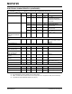
MCP4725 TABLE 7-1: I2C SERIAL TIMING SPECIFICATIONS Electrical Specifications: Unless otherwise specified, all limits are specified for TA = -40 to +85°C, VDD = +2.7V to +5.0V, VSS = 0V.
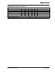
MCP4725 TABLE 7-1: I2C SERIAL TIMING SPECIFICATIONS (CONTINUED) Electrical Specifications: Unless otherwise specified, all limits are specified for TA = -40 to +85°C, VDD = +2.7V to +5.0V, VSS = 0V.
MCP4725 TF TSU:STA SCL TLOW SDA TR THIGH TSP THD:STA TSU:DAT THD:DAT TSU:STO TBUF 0.3VDD 0.7VDD TAA FIGURE 7-4: DS22039D-page 32 I2C Bus Timing Data. © 2009 Microchip Technology Inc.
MCP4725 TYPICAL APPLICATIONS The MCP4725 device is one of Microchip’s latest DAC device family with non-volatile EEPROM memory. The device is a general purpose resistive string DAC intended to be used in applications where a precision, and low power DAC with moderate bandwidth is required. Since the device includes non-volatile EEPROM memory, the user can use this device for applications that require the output to return to the previous set-up value on subsequent power-ups.
MCP4725 8.2 Using Non-Volatile EEPROM Memory The user can store the DAC input code (12 bits) and power-down configuration bits (2 bits) in the internal non-volatile EEPROM memory using the I2C write command. The user can also read the EEPROM data using the I2C read command. When the device is first powered after power is shut down, the device uploads the EEPROM contents to the DAC register automatically and provides the DAC output immediately.
MCP4725 8.5.2 DECREASING THE OUTPUT STEP SIZE output is scaled down by the factor of the ratio of the voltage divider. Note that the bypass capacitor on the output of the voltage divider plays a critical function in attenuating the output noise of the DAC and the induced noise from the environment. Calibrating the threshold of a diode, transistor or resistor may require a very small step size in the DAC output voltage. These applications may require about 200 µV of step resolution within 0.8V of range.
MCP4725 8.5.3 BUILDING A “WINDOW” DAC Some sensor applications require very high resolution around the set point or threshold voltage. Example 8-2 shows an example of creating a “window” around the threshold using a voltage divider network with a pull-up and pull-down resistor. In the circuit, the output voltage range is scaled down, but its step resolution is increased greatly. VDD MCP4725 R R 1 VOUT A0 6 2 VSS SCL 5 3 VDD SDA 4 0.
MCP4725 8.5.4 BIPOLAR OPERATION Bipolar operation is achievable using the MCP4725 by using an external operational amplifier (op amp). This allows a general purpose DAC, with its cost and availability advantages, to meet almost any desired output voltage range, power and noise performance. Example 8-3 illustrates a simple bipolar voltage source configuration. R1 and R2 allow the gain to be selected, while R3 and R4 shift the DAC's output to a selected offset.
MCP4725 8.5.4.1 Design a Bipolar DAC using Example 8-3 Some applications desires an output step magnitude of 1 mV with an output range of ±2.05V. The following steps explain the design solution: 1. 2. Calculate the range: +2.05V – (-2.05V) = 4.1V. Calculate the resolution needed: 4.1V/1 mV = 4100 steps Note that 212 = 4096 for 12-bit resolution. 3. The amplifier gain (R2/R1), multiplied by VDD, must be equal to the desired minimum output to achieve bipolar operation.
MCP4725 8.5.5 PROGRAMMABLE CURRENT SOURCE Example 8-3 illustrates an example how to convert the DAC voltage output to a digitally selectable current source by adding a voltage follower and a sensor register. VDD MCP4725 1 VOUT 2 VSS 3 VDD 0.
MCP4725 NOTES: DS22039D-page 40 © 2009 Microchip Technology Inc.
MCP4725 9.0 DEVELOPMENT SUPPORT 9.1 Evaluation & Demonstration Boards The MCP4725 SOT-23-6 Evaluation Board is available from Microchip Technology Inc. This board works with Microchip’s PICkit™ Serial Analyzer. The user can program the DAC input codes and EEPROM data, or read the programmed data using the easy to use PICkit Serial Analyzer with the Graphic User Interface software. Refer to www.microchip.com for further information on this product’s capabilities and availability.
MCP4725 NOTES: DS22039D-page 42 © 2009 Microchip Technology Inc.
MCP4725 10.0 PACKAGING INFORMATION 10.1 Package Marking Information 6-Lead SOT-23 Example Part Number XXNN 1 e3 Note: Code MCP4725A0T-E/CH A0 (00) AJNN MCP4725A1T-E/CH A1 (01) APNN MCP4725A2T-E/CH A2 (10) AQNN MCP4725A3T-E/CH A3 (11) ARNN Legend: XX...
MCP4725 / $ !$ % $ 0 $$ ,33... 3 " .
MCP4725 APPENDIX A: REVISION HISTORY Revision D (June 2009) The following is the list of modifications: 1. VDD_RAMP parameter in Section Added “ELECTRICAL CHARACTERISTICS” and description in Section 5.4.2 “VDD Ramp Rate and EEPROM”. Revision C (November 2007) The following is the list of modifications: 1. Corrected Address Options Identification System page. on Product Revision B (October 2007) The following is the list of modifications: 1. 2. 3. 4. Added characterization graphs to document.
MCP4725 NOTES: DS22039D-page 46 © 2009 Microchip Technology Inc.
MCP4725 PRODUCT IDENTIFICATION SYSTEM To order or obtain information, e.g., on pricing or delivery, refer to the factory or the listed sales office. PART NO. XX Device Address Options Device: Address Options: X X MCP4725: XX Tape and Temperature Reel Range /XX Package Single Channel 12-Bit DAC w/EEPROM Memory A2 A1 A0 * = 0 0 External A1 = 0 1 External A2 = 1 0 External A3 = 1 1 External a) b) A0 * Default option.
MCP4725 NOTES: DS22039D-page 48 © 2009 Microchip Technology Inc.
Note the following details of the code protection feature on Microchip devices: • Microchip products meet the specification contained in their particular Microchip Data Sheet. • Microchip believes that its family of products is one of the most secure families of its kind on the market today, when used in the intended manner and under normal conditions. • There are dishonest and possibly illegal methods used to breach the code protection feature.
WORLDWIDE SALES AND SERVICE AMERICAS ASIA/PACIFIC ASIA/PACIFIC EUROPE Corporate Office 2355 West Chandler Blvd. Chandler, AZ 85224-6199 Tel: 480-792-7200 Fax: 480-792-7277 Technical Support: http://support.microchip.com Web Address: www.microchip.