
Data Sheet

BSS138 Rev C(W)
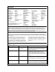
Electrical Characteristics T
A
= 25°C unless otherwise noted
Symbol Parameter Test Conditions Min Typ Max Units
Off Characteristics
BV
DSS
Drain–Source Breakdown Voltage
V
GS
= 0 V, I
D
= 250 µA
50 V
∆BV
DSS
∆T
J
Breakdown Voltage Temperature
Coefficient
I
D
= 250 µA,Referenced to 25°C
72
mV/°C
I
DSS
Zero Gate Voltage Drain Current V
DS
= 50 V, V
GS
= 0 V 0.5
µA
V
DS
= 50 V, V
GS
= 0 V T
J
= 125°C
5
µA
V
DS
= 30 V, V
GS
= 0 V 100 nA
I
GSS
Gate–Body Leakage.
V
GS
= ±20 V, V
DS
= 0 V
±100
nA
On Characteristics
(Note 2)
V
GS(th)
Gate Threshold Voltage V
DS
= V
GS
, I
D
= 1 mA 0.8 1.3 1.5 V
∆V
GS(th)
∆T
J
Gate Threshold Voltage
Temperature Coefficient
I
D
= 1 mA,Referenced to 25°C
–2
mV/°C
R
DS(on)
Static Drain–Source
On–Resistance
V
GS
= 10 V, I
D
= 0.22 A
V
GS
= 4.5 V, I
D
= 0.22 A
V
GS
= 10 V, I
D
= 0.22 A, T
J
= 125°C
0.7
1.0
1.1
3.5
6.0
5.8
Ω
I
D(on)
On–State Drain Current V
GS
= 10 V, V
DS
= 5 V 0.2 A
g
FS
Forward Transconductance V
DS
= 10V, I
D
= 0.22 A 0.12 0.5 S
Dynamic Characteristics
C
iss
Input Capacitance 27 pF
C
oss
Output Capacitance 13 pF
C
rss
Reverse Transfer Capacitance
V
DS
= 25 V, V
GS
= 0 V,
f = 1.0 MHz
6 pF
R
G
Gate Resistance V
GS
= 15 mV, f = 1.0 MHz 9
Ω
Switching Characteristics
(Note 2)
t
d(on)
Turn–On Delay Time 2.5 5 ns
t
r
Turn–On Rise Time 9 18 ns
t
d(off)
Turn–Off Delay Time 20 36 ns
t
f
Turn–Off Fall Time
V
DD
= 30 V, I
D
= 0.29 A,
V
GS
= 10 V, R
GEN
= 6 Ω
7 14 ns
Q
g
Total Gate Charge 1.7 2.4 nC
Q
gs
Gate–Source Charge 0.1 nC
Q
gd
Gate–Drain Charge
V
DS
= 25 V, I
D
= 0.22 A,
V
GS
= 10 V
0.4 nC
Drain–Source Diode Characteristics and Maximum Ratings
I
S
Maximum Continuous Drain–Source Diode Forward Current 0.22 A
V
SD
Drain–Source Diode Forward
Voltage
V
GS
= 0 V, I
S
= 0.44 A(Note 2) 0.8 1.4 V
Notes:
1. R
θJA
is the sum of the junction-to-case and case-to-ambient thermal resistance where the case thermal reference is defined as the solder mounting surface of
the drain pins. R
θJC
is guaranteed by design while R
θCA
is determined by the user's board design.
a) 350°C/W when mounted on a
minimum pad..
Scale 1 : 1 on letter size paper
2. Pulse Test: Pulse Width ≤ 300 µs, Duty Cycle ≤ 2.0%
BSS138