
Data Sheet

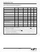

Si4702/03-C19
Rev. 1.1 5
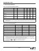
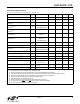
Table 3. DC Characteristics
1
(V
D
= V
A
= 2.7 to 3.6 V, V
IO
= 1.5 to 3.6 V, T
A
= –20 to 85 °C)
Parameter Symbol Test Condition Min Typ Max Unit
Analog Operating Supply Current
2
I
A
ENABLE = 1 — 10.8 — mA
Digital Operating Supply Current
2
I
D
ENABLE = 1 — 3.3 — mA
Interface Operating Supply
Current
2
I
IO
ENABLE = 1 — 0.3 — mA
Total Operating Supply
Current
2,3,4,5
I
OP
ENABLE = 1
Low SNR signal
— 15.3 16.8 mA
Total Operating Supply
Current
2,3,4
I
OP
ENABLE = 1 — 14.4 15.9 mA
Total Operating Supply
Current
2,3,4,6
I
OP
ENABLE = 1
RDS = 1
— 14.9 16.4 mA
Total Operating Supply
Current
2,3,4,6
I
OP
ENABLE = 1
RDS = 1,
Low SNR signal
— 15.8 16.8 mA
Analog Powerdown Supply Current
2,7
I
APD
ENABLE = 0 — 3.5 — µA
Digital Powerdown Supply Current
2,7
I
DPD
ENABLE = 0 — 2.5 — µA
Interface Powerdown Supply
Current
2,7
I
IOPD
ENABLE = 0
SCLK, RCLK inactive
—2.5—µA
Total Powerdown Supply Current
2,7
I
PD
ENABLE = 0 — 8.5 12.0 µA
High Level Input Voltage
8
V
IH
0.7 x V
IO
—V
IO
+0.3 V
Low Level Input Voltage
8
V
IL
–0.3 — 0.3 x V
IO
V
High Level Input Current
8
I
IH
V
IN
= V
IO
= 3.6 V –10 — 10 µA
Low Level Input Current
8
I
IL
V
IN
= 0 V,
V
IO
= 3.6 V
–10 — 10 µA
High Level Output Voltage
9
V
OH
I
OUT
= 500 µA 0.8 x V
IO
——V
Low Level Output Voltage
9
V
OL
I
OUT
= –500 µA — — 0.2 x V
IO
V
Notes:
1. All specifications for the Si4702 unless otherwise noted.
2. Refer to Register 02h, "Power Configuration" on page 24 for ENABLE bit description.
3. The LNA is automatically switched to higher current mode for optimum sensitivity in low SNR conditions.
4. Analog and digital supply currents are simultaneously adjusted based on SNR level.
5. Stereo and RDS functionality are disabled at low SNR levels.
6. RDS functionality only available for Si4703.
7. Refer to Section 4.9. "Reset, Powerup, and Powerdown" on page 19.
8. For input pins SCLK, SEN
, SDIO, RST, RCLK, GPIO1, GPIO2, and GPIO3.
9. For output pins SDIO, GPIO1, GPIO2, and GPIO3.